P4C1024-17P3I Просмотр технического описания (PDF) - Semiconductor Corporation
Номер в каталоге
Компоненты Описание
Список матч
P4C1024-17P3I Datasheet PDF : 14 Pages
| |||
P4C1024
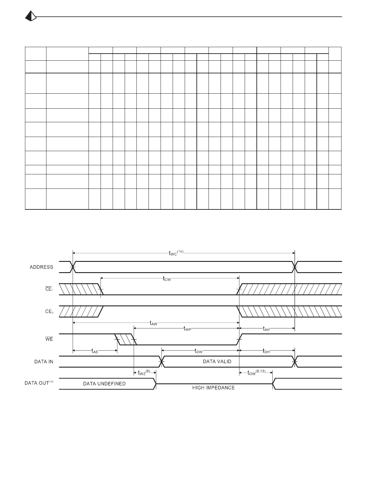
AC CHARACTERISTICS—WRITE CYCLE
(VCC = 5V ± 10%, All Temperature Ranges)(2)
Symbol
Parameter
-15
Min Max
-20
Min Max
-25
Min Max
-35
Min Max
-45
Min Max
-55
Min Max
-70
Min Max
-85
Min Max
-100
Min Max
-120
Min Max
Unit
tWC Write Cycle Time 15
20
25
35
45
55
70
85
100
120
ns
Chip Enable
tCW Time to End of 12
15
18
22
30
35
45
50
60
75
ns
Write
tAW
Address Valid to
End of Write
12
15
20
25
35
45
60
70
85
100
ns
tA S
Address Set-up
Time
0
0
0
0
0
0
0
0
0
0
ns
tWP
Write Pulse
Width
12
15
18
22
25
30
40
45
55
70
ns
tA H
Address Hold
Time
0
0
0
0
0
0
0
0
0
0
ns
tDW
Data Valid to
End of Write
7
8
10
15
20
25
30
35
45
60
ns
tDH Date Hold Time 0
0
0
0
0
0
0
0
0
0
ns
tWZ
Write Enable to
Output in High Z
8
10
11
15
18
20
25
30
40
50 ns
Output Active
tOW from End of
3
3
3
3
3
3
3
3
3
3
ns
Write
TIMING WAVEFORM OF WRITE CYCLE NO. 1 (WE CONTROLLED)(11)
Notes:
11. CE1 and WE must be LOW, and CE2 HIGH for WRITE cycle.
12. OE is LOW for this WRITE cycle to show tWZ and tOW.
13. If CE1 goes HIGH, or CE2 goes LOW, simultaneously with WE HIGH,
the output remains in a high impedance state.
14. Write Cycle Time is measured from the last valid address to the first
transitioning address.
Document # SRAM124 REV A
Page 6 of 14
Share Link: 