OZ965 Просмотр технического описания (PDF) - Unspecified
Номер в каталоге
Компоненты Описание
Список матч
OZ965 Datasheet PDF : 7 Pages
| |||
OZ965
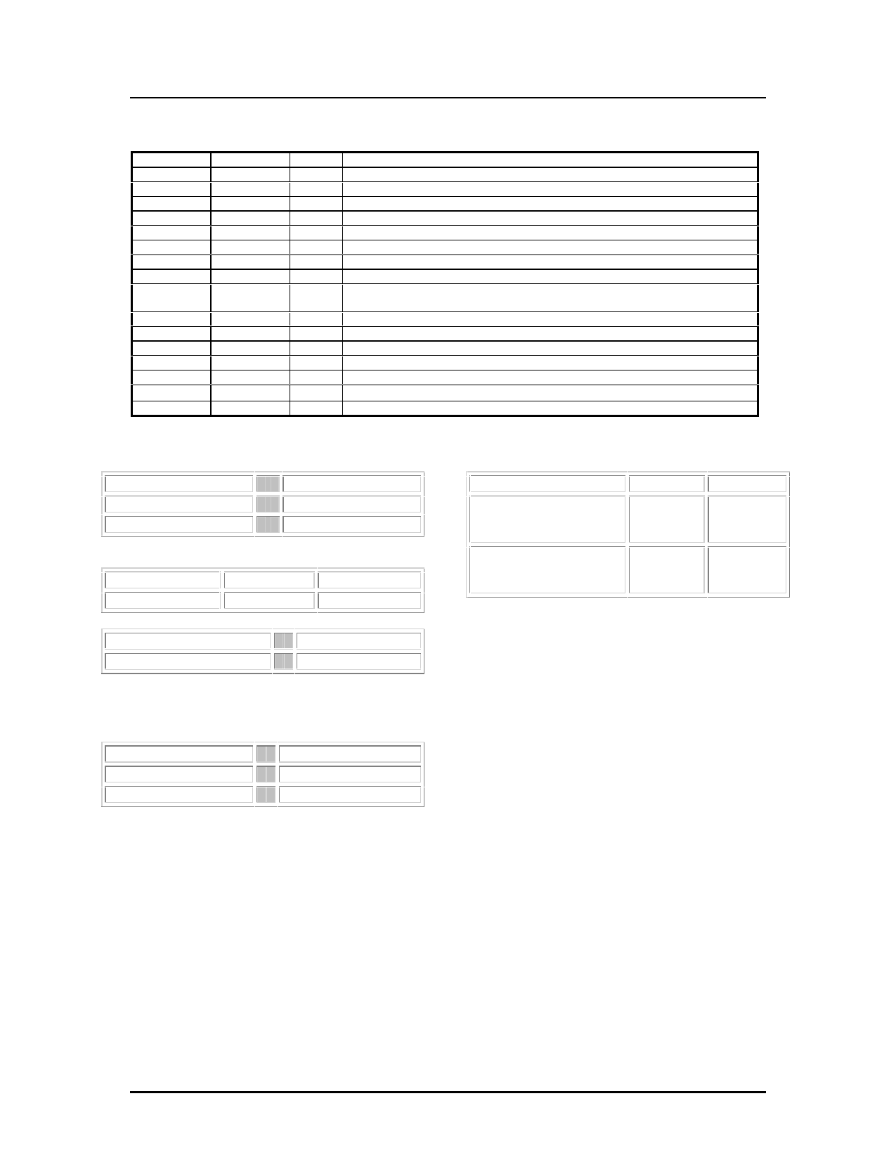
PIN DESCRIPTION
Names
REF
HCLMP
LCLMP
SCP
ADJ
FB
CMP
GND
SST
PDR
NDR
ENA
OPS
CT
RT
VDD
Pin No.
1
2
3
4
5
6
7
8
9
10
11
12
13
14
15
16
I/O
O
I
I
I
I
I
O
GND
I
O
O
I
I
I/O
I/O
PWR
Description
Reference voltage output. Nominal voltage is 2.5 V.
Clamping maximum duty cycle under normal operation.
Clamping maximum duty cycle under open-lamp condition.
Short-circuit protection input (VTH=0.6V)
Reference voltage input for dimming control.
Current sense feedback.
Compensation for the current sense feedback.
Ground.
Soft-start ensures lamp current pulses gradually increases to its normal
value
Gate drive output for the P-MOSFET.
Gate drive output for the N-MOSFET.
Enable input, active high (VTH=1.5V)
Output current sense (VTH=0.6V)
Timing capacitor. CT and RT set the clock frequency.
Timing resistor. Fosc = 1.91 / (Rt • Ct)
Supply voltage input.
ABSOLUTE MAXIMUM RATINGS
VDD
GND
Logic inputs
5.5V
+/- 0.3V
-0.3 V to VDD+0.3V
Operating temp.
OZ965
0oC to 70oC
OZ965I
-40oC to 85oC
Power dissipation
- 16-pin SOP
- 16-pin TSSOP
Thermal Impedance
- 16-pin SOP
- 16-pin TSSOP
OZ965
.720W
.690W
111oC/W
115oC/W
OZ965I
.580W
.550W
111oC/W
115oC/W
Operating junction temp.
Storage temp.
150oC
-55oC to 150oC
RECOMMENDED OPERATING RANGE
VDD
Fosc
Rosc
5.0 V +/- 5%
30 KHz to 200 KHz
50 k to 150 k
OZ965-SF-3.0
Page 3
Share Link: 