W91550DNH Просмотр технического описания (PDF) - Winbond
Номер в каталоге
Компоненты Описание
Список матч
W91550DNH Datasheet PDF : 32 Pages
| |||
W91550DN SERIES
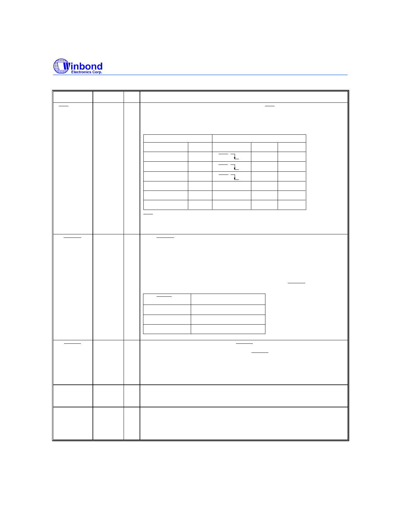
Pin Description, continued
SYMBOL PIN
HFI , HFO 57, 58
LOCK
64
I/O
FUNCTION
I, O Handfree control pins. A low pulse on the HFI input pin toggles the
handfree control state.
Status of the handfree control is listed in the following table:
CURRENT STATE
Hook SW.
HFO
−
Low
On Hook
High
Off Hook
High
On Hook
−
Off Hook
Low
Off Hook
High
NEXT STATE
Input
HFO
HFI
High
HFI
Low
HFI
Low
Off Hook
Low
On Hook
Low
On Hook
High
Dialing
Yes
No
Yes
Yes
No
Yes
HFI pin is pulled to VDD by internal resistor.
Detailed timing diagram is shown in Figure 4.
I The LOCK pin is used to prevent "0" or "9" dialing under PABX
system long distance call control. When the first key input after reset
is "0" or "9", all the key inputs, including "0" or "9" key, become
invalid, and the chip generates no output.
The telephone is reinitialized by a reset.
The following table describes the functions of the LOCK pin:
LOCK PIN
Floating
VDD
VSS
FUNCTION
Normal dialing
"0", "9" dialing inhibited
"0" dialing inhibited
TEST
VLCD
CP, CN
37
59
60, 61
I In normal operation, pulling the TEST pin to VDD inhibits the single
tone. In testing operation, pulling the TEST pin to VSS enables a
single tone to be created by pressing two keys simultaneously, and all
of the timing parameters for pulse dialing are faster than in normal
operation.
I Power supply pin for LCD driver.
A 1µF capacitor is connected between VLCD and VSS.
I CP is the voltage control capacitor positive pin.
CN is the voltage control capacitor negative pin.
A 1 µF capacitor is connected between these two pins.
Publication Release Date: November 1997
-5-
Revision A3
Share Link: 