HI2315JCQ Просмотр технического описания (PDF) - Intersil
Номер в каталоге
Компоненты Описание
Список матч
HI2315JCQ Datasheet PDF : 9 Pages
| |||
HI2315
Pin Descriptions (Continued)
PIN NO.
SYMBOL
15, 27
25
17
DVSS
AVSS
IREF
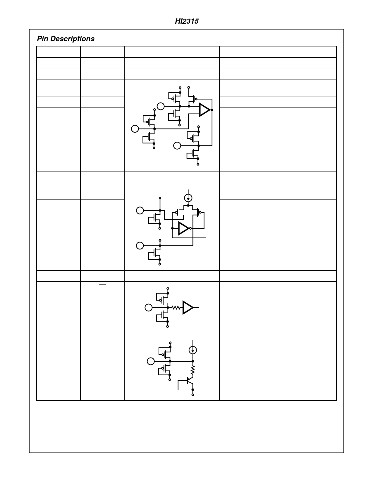
EQUIVALENT CIRCUIT
AVDD
AVDD
19
VREF
22
VG
AVDD 17
+
-
AVSS
AVDD
19
DESCRIPTION
Digital GND.
Analog GND.
Connect resistance “16R” which is 16 times output
resistance “R”.
Sets output full scale value.
Connect a capacitor of approximately 0.1µF.
20, 21
24
23
AVDD
IO
IO
AVSS
22
AVSS
AVDD
24
Analog VDD.
Current Output pin. Output can be retrieved by
connecting resistance. The standard is 200Ω.
Inverted Current Output pin. Connect to GND
normally.
13, 28
11
18
DVDD
CE
SREF
AVSS
AVDD
23
AVSS
DVDD
11
DVSS
AVDD
18
AVSS
Digital VDD.
Chip Enable pin. No signal (0V output) at high makes
power consumption minimum.
Independent Constant-Voltage Source Output pin
using band gap reference. Stable voltage
independent of the fluctuation for supply voltage can
be obtained by connecting to VREF. See Application
Circuit 2 for details.
10-3
Share Link: 