NLX2G08(2009) Просмотр технического описания (PDF) - ON Semiconductor
Номер в каталоге
Компоненты Описание
Список матч
NLX2G08 Datasheet PDF : 5 Pages
| |||
NLX2G08
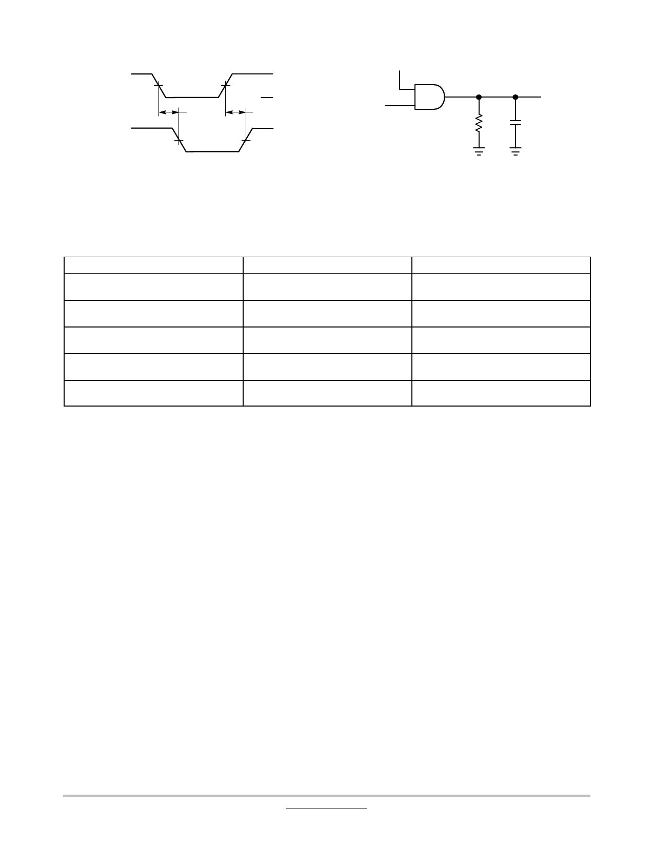
VCC
INPUT 50%
An and Bn
OUTPUT Yn
tPLH
50% VCC
50% VCC
GND
tPHL
VOH
VOL
RL
CL
A 1−MHz square input wave is recommended for
propagation delay tests.
Figure 3. Switching Waveform
Figure 4. Test Circuit
DEVICE ORDERING INFORMATION
Device Order Number
NLX2G08MUTCG
Package Type
UQFN8
(Pb−Free)
Tape and Reel Size†
3000 Unit / Tape & Reel
†For information on tape and reel specifications, including part orientation and tape sizes, please refer to our Tape and Reel Packaging
Specifications Brochure, BRD8011/D.
http://onsemi.com
4
Share Link: 