NM24C08U Просмотр технического описания (PDF) - Fairchild Semiconductor
Номер в каталоге
Компоненты Описание
Список матч
NM24C08U Datasheet PDF : 13 Pages
| |||
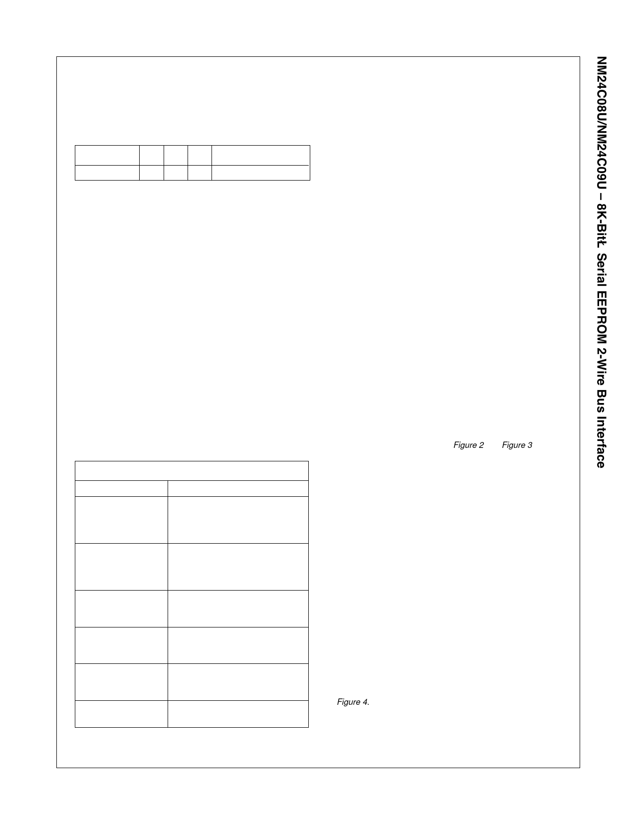
Device Operation Input (A2)
Device address pin A2 is connected to VCC or VSS to configure
the EEPROM chip address. Table 1 shows the active pin.
Table 1.
Device
A0 A1 A2 Effects of Addresses
NM24C08U/09U x x ADR 21 = 2; 2 x (4 x 2k) = 16K
Background Information (IIC Bus)
As mentioned, the IIC bus allows synchronous bidirectional com-
munication between Transmitter/Receiver using the SCL (clock)
and SDA (Data I/O) lines. All communication must be started with
a valid START condition, concluded with a STOP condition and
acknowledged by the Receiver with an ACKNOWLEDGE condi-
tion.
As shown below, the EEPROMs on the IIC bus may be configured
in any manner required, the total memory addressed can not
exceed 16K (16,384 bits). EEPROM memory address program-
ming is controlled by 2 methods:
• Hardware configuring the A2 pin (Device Address pin) with
pull-up or pull-down to VCC or VSS. All unused pins must be
grounded (tied to VSS).
• Software addressing the required PAGE BLOCK within the
device memory array (as sent in the Slave Address string).
For devices with densities greater than 16K, a different protocol,
the Extended IIC protocol, is used. Refer to NM24C32U datasheet
(for example) for additional details.
Addressing an EEPROM memory location involves sending a
command string with the following information:
[DEVICE TYPE]–[DEVICE ADDRESS]–[PAGE BLOCK AD-
DRESS]–[BYTE ADDRESS]
BYTE
PAGE
PAGE BLOCK
MASTER
SLAVE
TRANSMITTER
RECEIVER
DEFINITIONS
8 bits (byte) of data
16 sequential addresses (one byte
each) that may be programmed
during a 'Page Write' programming
cycle
2048 (2K) bits organized into 16
pages of addressable memory.
(8 bits) x (16 bytes) x (16 pages)
= 2048 bits
Any IIC device CONTROLLING the
transfer of data (such as a
microprocessor)
Device being controlled
(EEPROMs are always considered
Slaves)
Device currently SENDING data on
the bus (may be either a Master or
Slave).
Device currently RECEIVING data
on the bus (Master or Slave)
Pin Descriptions
Serial Clock (SCL)
The SCL input is used to clock all data into and out of the device.
Serial Data (SDA)
SDA is a bidirectional pin used to transfer data into and out of the
device. It is an open drain output and may be wire–ORed with any
number of open drain or open collector outputs.
WP Write Protection (NM24C09U Only)
If tied to VCC, PROGRAM operations onto the upper half of the
memory will not be executed. READ operations are possible. If
tied to VSS, normal operation is enabled, READ/WRITE over the
entire memory is possible.
This feature allows the user to assign the upper half of the memory
as ROM which can be protected against accidental programming.
When write is disabled, slave address and word address will be
acknowledged but data will not be acknowledged.
Device Operation
The NM24C08U/09U supports a bidirectional bus oriented proto-
col. The protocol defines any device that sends data onto the bus
as a transmitter and the receiving device as the receiver. The
device controlling the transfer is the master and the device that is
controlled is the slave. The master will always initiate data
transfers and provide the clock for both transmit and receive
operations. Therefore, the NM24C08U/09U will be considered a
slave in all applications.
Clock and Data Conventions
Data states on the SDA line can change only during SCL LOW.
SDA state changes during SCL HIGH are reserved for indicating
start and stop conditions. Refer to Figure 2 and Figure 3 on next
page.
Start Condition
All commands are preceded by the start condition, which is a
HIGH to LOW transition of SDA when SCL is HIGH. The
NM24C08U/09U continuously monitors the SDA and SCL lines for
the start condition and will not respond to any command until this
condition has been met.
Stop Condition
All communications are terminated by a stop condition, which is a
LOW to HIGH transition of SDA when SCL is HIGH. The stop
condition is also used by the NM24C08U/09U to place the device
in the standby power mode.
Write Cycle Timing
Acknowledge
Acknowledge is a hardware convention used to indicate success-
ful data transfers. The transmitting device, either master or slave,
will release the bus after transmitting eight bits.
During the ninth clock cycle the receiver will pull the SDA line to
LOW to acknowledge that it received the eight bits of data. Refer
to Figure 4.
7
NM24C08U/09U Rev. B.1
www.fairchildsemi.com
Share Link: 