MX93032 Просмотр технического описания (PDF) - Macronix International
Номер в каталоге
Компоненты Описание
Список матч
MX93032 Datasheet PDF : 69 Pages
| |||
MX93032
Decision Rules between MCU mode and DSP Mode:
1. The contents located on 0xE000 and 0xE001 are 0x1234 and 0x5678, It will be considered as external DSP mode.
This configuration is used for developing customer’s control codes on MXIC’s MX93032-M1 IC with standard
code.
2. The contents located on 0x680E and 0x680F are 0x5678 and 0xA988, it will be considered as MCU mode. This is
the only one configuration for MCU mode under developing and mass production.
3. Either the content located on 0x680E and not 0x5678 or that located on 0x680F are not 0xA988, it will be consid-
ered as DSP mode. The configuration is used for mass production for DSP mode adopted.
4. The decision priority depends on the items order. That is, the item labeled with smaller number has higher priority.
CONTROL CODE CONFIGURATION (DSP MODE)
There are two configurations for customer development or production.
Configuration 1 :
In this configuration, the BIOS+ALGORITHM and control codes are all running in the external high-speed EPROMs
or SRAMs. The MX93032-M1 pin 97 (EROM) must be set to high.
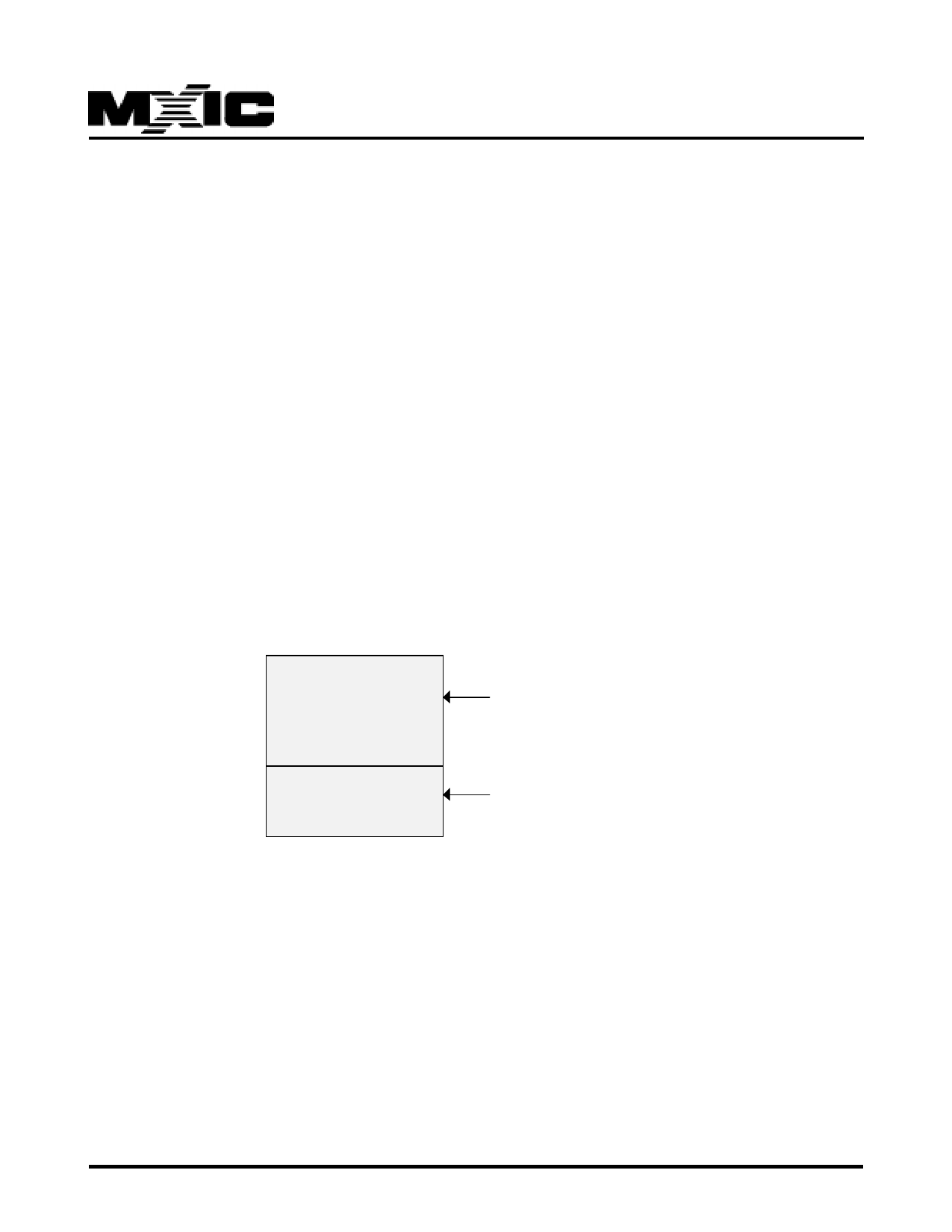
External high-speed EPROMs or SRAMs
0000H
26K words
BIOS+ALGORITHM c
(address 0000H - 67F
6800H
7F FFH
6K words
control code
(address 6800H - 7F
This configuration is mainly used in the development stage and the access time of high-speed EPROMs or SRAMs
must be less than 30ns.
P/N:PM0689
REV. 1.0.3, DEC. 13, 1999
10
Share Link: 