CY7C1329-60AC Просмотр технического описания (PDF) - Cypress Semiconductor
Номер в каталоге
Компоненты Описание
Список матч
CY7C1329-60AC Datasheet PDF : 14 Pages
| |||
CY7C1329
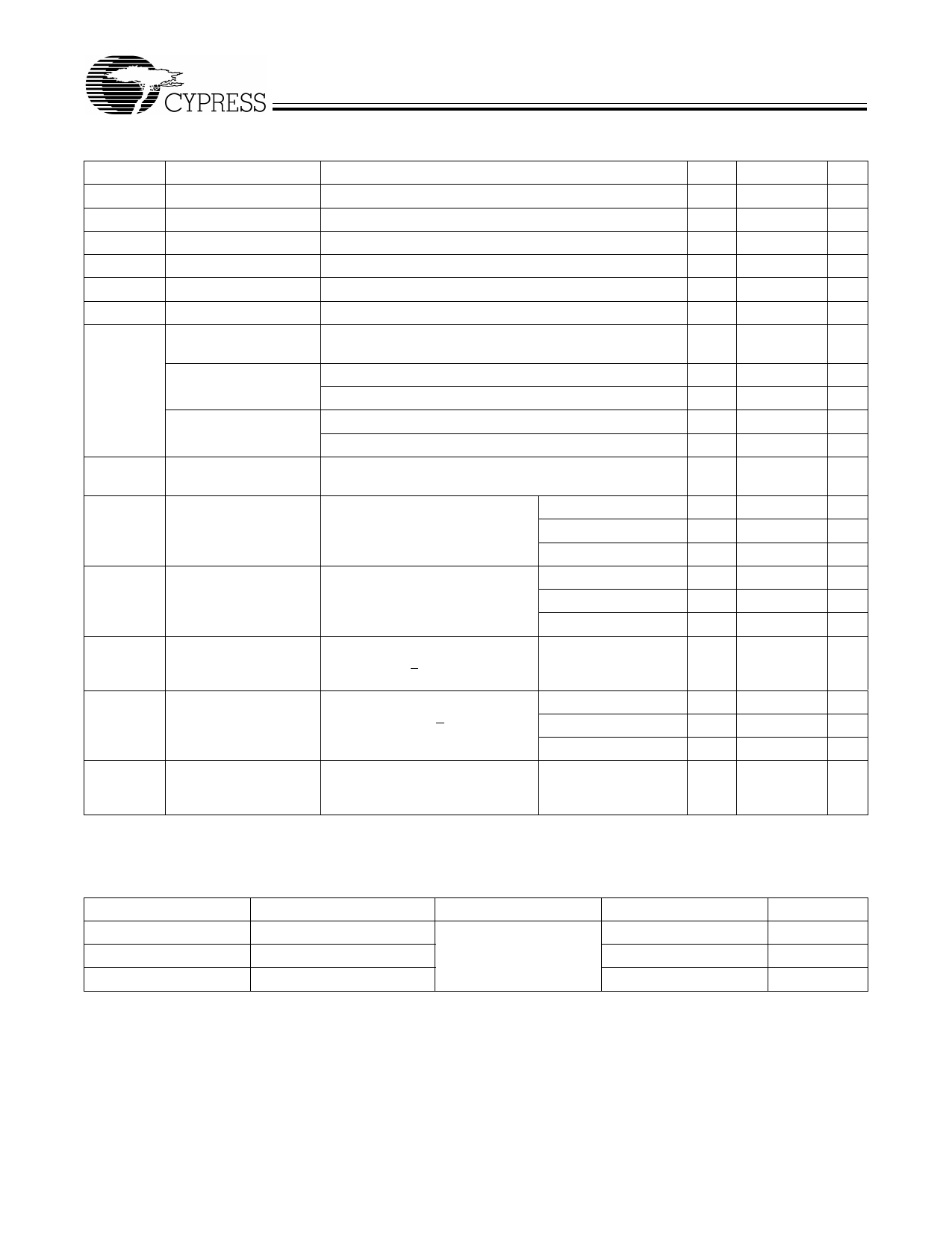
Electrical Characteristics Over the Operating Range
Parameter
Description
Test Conditions
Min.
Max.
Unit
VDD
VDDQ
VOH
VOL
VIH
VIL
IX
Power Supply Voltage
I/O Supply Voltage
Output HIGH Voltage
Output LOW Voltage
Input HIGH Voltage
Input LOW Voltage[7]
Input Load Current
except ZZ and MODE
3.3V −5%/+10%
3.3V −5%/+10%
VDD = Min., IOH = −4.0 mA
VDD = Min., IOL = 8.0 mA
GND ≤ VI ≤ VDDQ
3.135
3.6
V
3.135
3.6
V
2.4
V
0.4
V
2.0 VDDQ + 0.3V V
–0.3
0.8
V
−5
5
µA
Input Current of MODE Input = VSS
Input = VDDQ
Input Current of ZZ
Input = VSS
Input = VDDQ
IOZ
Output Leakage
GND ≤ VI ≤ VDDQ, Output Disabled
Current
–30
µA
5
µA
–5
µA
30
µA
−5
5
µA
IDD
VDD Operating Supply VDD = Max., IOUT = 0 mA,
7.5-ns cycle, 133 MHz
Current
f = fMAX = 1/tCYC
10-ns cycle, 100 MHz
325
mA
260
mA
13.3-ns cycle, 75 MHz
260
mA
ISB1
Automatic CS
Max. VDD, Device Deselected, 7.5-ns cycle, 133 MHz
Power-Down
Current—TTL Inputs
VIN ≥ VIH or VIN ≤ VIL
f = fMAX = 1/tCYC
10-ns cycle, 100 MHz
13.3-ns cycle, 75 MHz
60
mA
50
mA
50
mA
ISB2
Automatic CS
Max. VDD, Device Deselected, VIN All speeds
Power-Down
≤ 0.3V or VIN > VDDQ – 0.3V, f = 0
Current—CMOS Inputs
5
mA
ISB3
Automatic CS
Max. VDD, Device Deselected, or 7.5-ns cycle, 133 MHz
Power-Down
VIN ≤ 0.3V or VIN > VDDQ – 0.3V
Current—CMOS Inputs f = fMAX = 1/tCYC
10-ns cycle, 100 MHz
13.3-ns cycle, 75 MHz
40
mA
30
mA
30
mA
ISB4
Automatic CS
Max. VDD, Device Deselected,
Power-Down
VIN ≥ VIH or VIN ≤ VIL, f = 0
Current—TTL Inputs
25
mA
Capacitance[9]
Parameter
Description
Test Conditions
CIN
CCLK
CI/O
Input Capacitance
Clock Input Capacitance
Input/Output Capacitance
TA = 25°C, f = 1 MHz,
VDD = 3.3V,
VDDQ = 3.3V
Note:
9. Tested initially and after any design or process changes that may affect these parameters.
Max.
4
4
4
Unit
pF
pF
pF
7
Share Link: 