MT5C2561 Просмотр технического описания (PDF) - Austin Semiconductor
Номер в каталоге
Компоненты Описание
Список матч
MT5C2561 Datasheet PDF : 11 Pages
| |||
Austin Semiconductor, Inc.
SRAM
MT5C2561
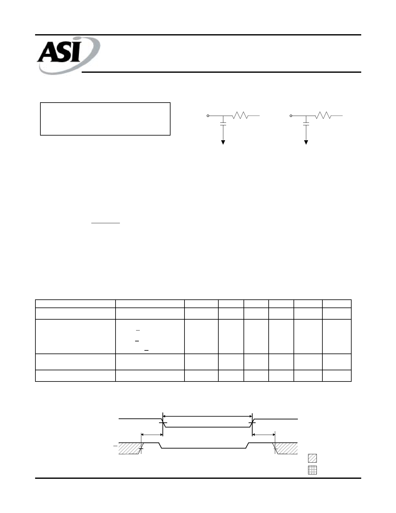
AC TEST CONDITIONS
Input pulse levels ...................................... Vss to 3.0V
Input rise and fall times ......................................... 5ns
Input timing reference levels ................................ 1.5V
Output reference levels ....................................... 1.5V
Output load ................................. See Figures 1 and 2
167Ω
167Ω
Q
30pF VTH = 1.73V Q
5pF VTH = 1.73V
Fig. 1 Output Load
Equivalent
Fig. 2 Output Load
Equivalent
NOTES
1. All voltages referenced to VSS (GND).
2. -3V for pulse width < 20ns
3. ICC is dependent on output loading and cycle rates.
The specified value applies with the outputs
unloaded, and f = 1 Hz.
tRC (MIN)
4. This parameter is guaranteed but not tested.
5. Test conditions as specified with the output loading
as shown in Fig. 1 unless otherwise noted.
6. tLZCE, tLZWE, tLZOE, tHZCE, tHZOE and tHZWE are
specified with CL = 5pF as in Fig. 2. Transition is
measured ±200mV typical from steady state voltage,
allowing for actual tester RC time constant.
7. At any given temperature and voltage condition, tHZCE is
less than tLZCE, and tHZWE is less than tLZWE and tHZOE is
less than tLZOE.
8. WE\ is HIGH for READ cycle.
9. Device is continuously selected. Chip enable is held in
its active state.
10. Address valid prior to, or coincident with, latest
occurring chip enable.
11. tRC = Read Cycle Time.
12. Chip enable (CE\) and write enable (WE\) can initiate and
terminate a WRITE cycle.
DATA RETENTION ELECTRICAL CHARACTERISTICS (L Version Only)
DESCRIPTION
CONDITIONS
SYM MIN MAX UNITS
VCC for Retention Data
VDR
2
---
V
NOTES
Data Retention Current
CE\ > (VCC - 0.2V)
VIN > (VCC - 0.2V)
or < 0.2V
VCC = 2V ICCDR
900
µA
Chip Deselect to Data
Retention Time
tCDR
0
---
ns
4
Operation Recovery Time
tR
tRC
ns
4, 11
MT5C2561
Rev. 2.5 1/01
LOW Vcc DATA RETENTION WAVEFORM
VCC
tCDR
CE\
VIH
VIL
111122223333444455556666777788889999
DATA RETENTION MODE
4.5V
VDR > 2V
4.5V
VDR
tR
111122223333444455556666111177772111122288883222233343343344
111122223333DON’T CARE
1111222233334444UNDEFINED
Austin Semiconductor, Inc. reserves the right to change products or specifications without notice.
5
Share Link: 