MSM7543 Просмотр технического описания (PDF) - Oki Electric Industry
Номер в каталоге
Компоненты Описание
Список матч
MSM7543 Datasheet PDF : 19 Pages
| |||
¡ Semiconductor
MSM7543/7544
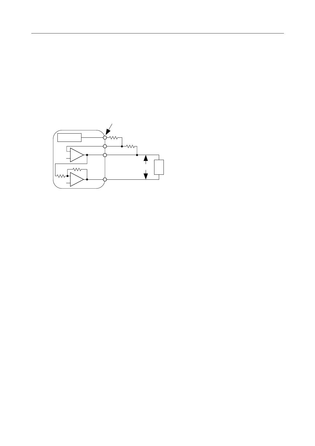
PWI, AOUT+, AOUT–
PWI is connected to the inverting input of the receive driver. The receive driver output is
connected to the AOUT– pin. Therefour, the receive level can be adjusted with the pins VFRO,
PWI, and AOUT–. When the PWI pin is not used, connect the PWI pin to the AOUT– pin, and
leave open the pins AOUT– and AOUT+. The output of AOUT+ is inverted with respect to the
output of AOUT–. Since the signal from which provides differential drive of an impedance of 1.2
kW, these outputs can directly be connected to a receiver of handset using a piezoelectric
earphone. Refer to the application example.
VI
Receive Filter
VFRO R6
PWI
R7
–
SG +
AOUT–
VO ZL
–
SG +
AOUT+
R6 > 20 kW
ZL ≥ 1.2 kW
Gain = VO/VI = 2 ¥ R7/R6 £ 2
During power saving and power down modes, the outputs of AOUT+ and AOUT– are in a high
impedance state .
The electrical driving capability of the AOUT– pin and AOUT+ pin is ±1.3 V maximum. The
output load resistor has a minimum value of 0.6 kW.
If an output amplitude less than ±1.3 V is allowed, these outputs can drive a load resistance less
than that described above.
For more details, refer to SINGLE POWER SUPPLY PCM CODEC APPLICATION NOTE.
VDD
Power supply pin for +5 V.
PCMIN
PCM signal input.
A serial PCM signal input to this pin is converted to an analog signal in synchronization with the
RSYNC signal and BCLOCK signal.
The data rate of the PCM signal is equal to the frequency of the BCLOCK signal.
The PCM signal is shifted at a falling edge of the BCLOCK signal and latched into the internal
register when shifted by eight bits.
The start of the PCM data (MSD) is identified at the rising edge of RSYNC.
BCLOCK
Shift clock signal input for the PCMIN and PCMOUT signal.
The frequency, equal to the data rate, is 64, 96, 128, 192, 256, 384, 512, 768, 1024, 1536, 1544, 2048,
or 200 kHz. Setting this signal to logic "1" or "0" drives both transmit and receive circuits to the
power saving state.
5/19
Share Link: 