MSM7544RS Просмотр технического описания (PDF) - Oki Electric Industry
Номер в каталоге
Компоненты Описание
Список матч
MSM7544RS Datasheet PDF : 19 Pages
| |||
¡ Semiconductor
MSM7543/7544
PIN AND FUNCTIONAL DESCRIPTIONS
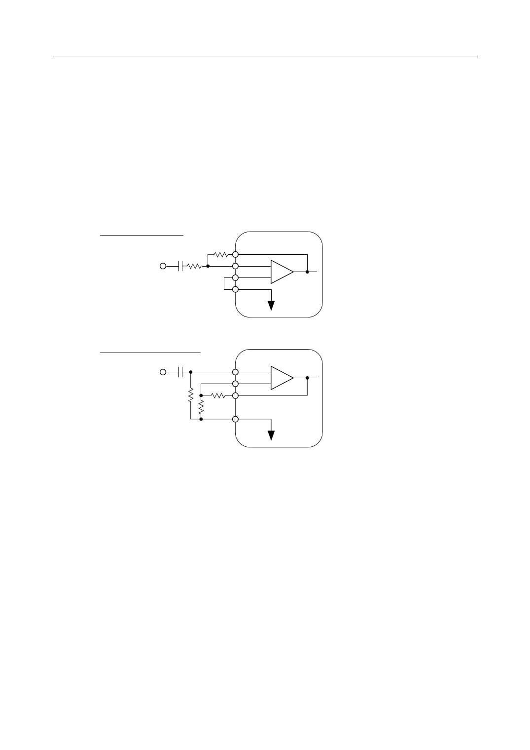
AIN+, AIN–, GSX
Transmit analog input and transmit level adjustment.
AIN+ is a non-inverting input to the op-amp; AIN– is an inverting input to the op-amp; GSX is
connected to the output of the op-amp and is used to adjust the level, as shown below.
When not using AIN– and AIN+, connect AIN– to GSX and AIN+ to SG. During power saving
and power down modes, the GSX output is at AG voltage.
1) Inverting input type
Analog input
C1
R1
GSX
R2
AIN–
AIN+
SG
–
+
R1 : variable
R2 > 20 kW
C1 > 1/(2 ¥ 3.14 ¥ 30 ¥ R1)
Gain = R2/R1 £ 10
2) Non inverting input type
C2
Analog input
R5
R4
R3
AIN+
AIN–
+
–
GSX
SG
R3 > 20 kW
R4 > 20 kW
R5 > 50 kW
C2 > 1/ (2 ¥ 3.14 ¥ 30 ¥ R5)
Gain = 1 + R4 / R3 £ 10
AG
Analog signal ground.
VFRO
Receive filter output.
The output signal has an amplitude of 2.4 VPP above and below the signal ground voltage (SG)
when the digital signal of +3 dBmO is input to PCMIN and can drive a load of 20 kW or more.
For driving a load of 20 kW or less, connect a resistor of 20 kW or more between the pins VFRO
and PWI.
When adding the frequency characteristics to the receive signal, refer to the application example.
During power saving or power down mode, the output of VFRO is at the voltage level of AG.
4/19
Share Link: 