MSM7512 Просмотр технического описания (PDF) - Oki Electric Industry
Номер в каталоге
Компоненты Описание
Список матч
MSM7512 Datasheet PDF : 12 Pages
| |||
Semiconductor
MSM7512B
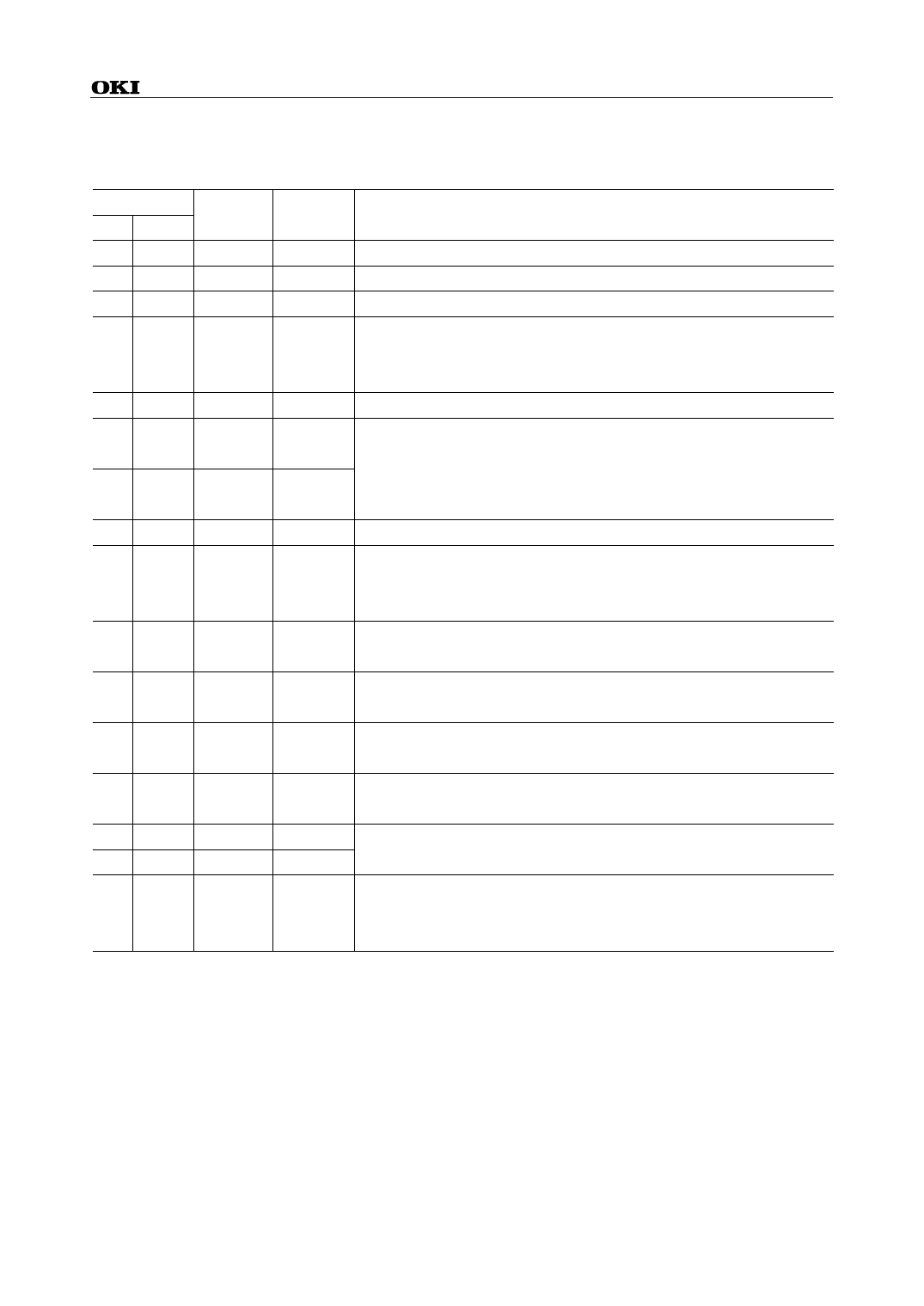
PIN DESCRIPTION
No.
RS GS-VK
1
1
2
3
3
5
Name
VDD
AI
AO
4
6
EAI
5
7
GND
6
8
X1
7 10
X2
8 12
CLK
9 13
RD
10 15
11 17
12 18
13 19
14 20
15 22
16 24
CD
XD
RS
TEST
MOD1
MOD2
AOG
I/O
Description
—
+3 V to +5 V Power Supply
I
Analog receive signal input.
O
Analog transmit signal output.
External analog signal input.
I
The signal applied to this pin is transmitted from AO via transmit output
amplifier. When not using this pin, it should be left open.
—
Ground, 0 V.
3.579545 MHz crystal resonator should be connected to X1 and X2.
I
When applying external clock 3.579545 MHz to the device, it should be
applied to X2 (not X1) via an AC-coupling capacitor of 100 pF and X1
O
has to be opened.
O
3.579545 MHz clock signal output.
Modem receive serial data output.
O
Digital "1" and "0" correspond to "Mark" and "Space", respectively. When
CD (Carrier Detect) is off, RD is held at "Mark" state.
FSK Receive signal and answer tone detect.
O
Digital "0" and "1" represent "Detect" and "Non-detect", respectively.
Modem transmit serial data input.
I*
Digital "1" and "0" correspond to "Mark" and "Space", respectively.
FSK signal and answer tone transmit enable.
I*
When digital "0" is applied to RS, transmitting becomes enable.
Chip test input.
I*
TEST should be open or digital "1".
I*
Operation mode select.
I*
Refer to Table 1.
Analog transmit signal amplitude select.
I*
Digital "1" Æ –10 dBm Typ. at AO
Digital "0" Æ –4 dBm Typ. at AO
Note : I* : Internally pulled-up input pin.
4/12
Share Link: 