MSM6948 Просмотр технического описания (PDF) - Oki Electric Industry
Номер в каталоге
Компоненты Описание
Список матч
MSM6948 Datasheet PDF : 13 Pages
| |||
¡ Semiconductor
MSM6948/6948V
Name
RD
RT
CF
CT
FT
VDD
Description
Demodulated serial data output.
This data is synchronized with the re-generated timing clock RT.
Receive data timing clock output.
This signal is re-generated by internal digital PLL.
Synchronizing to falling edge of RT, RD is output.
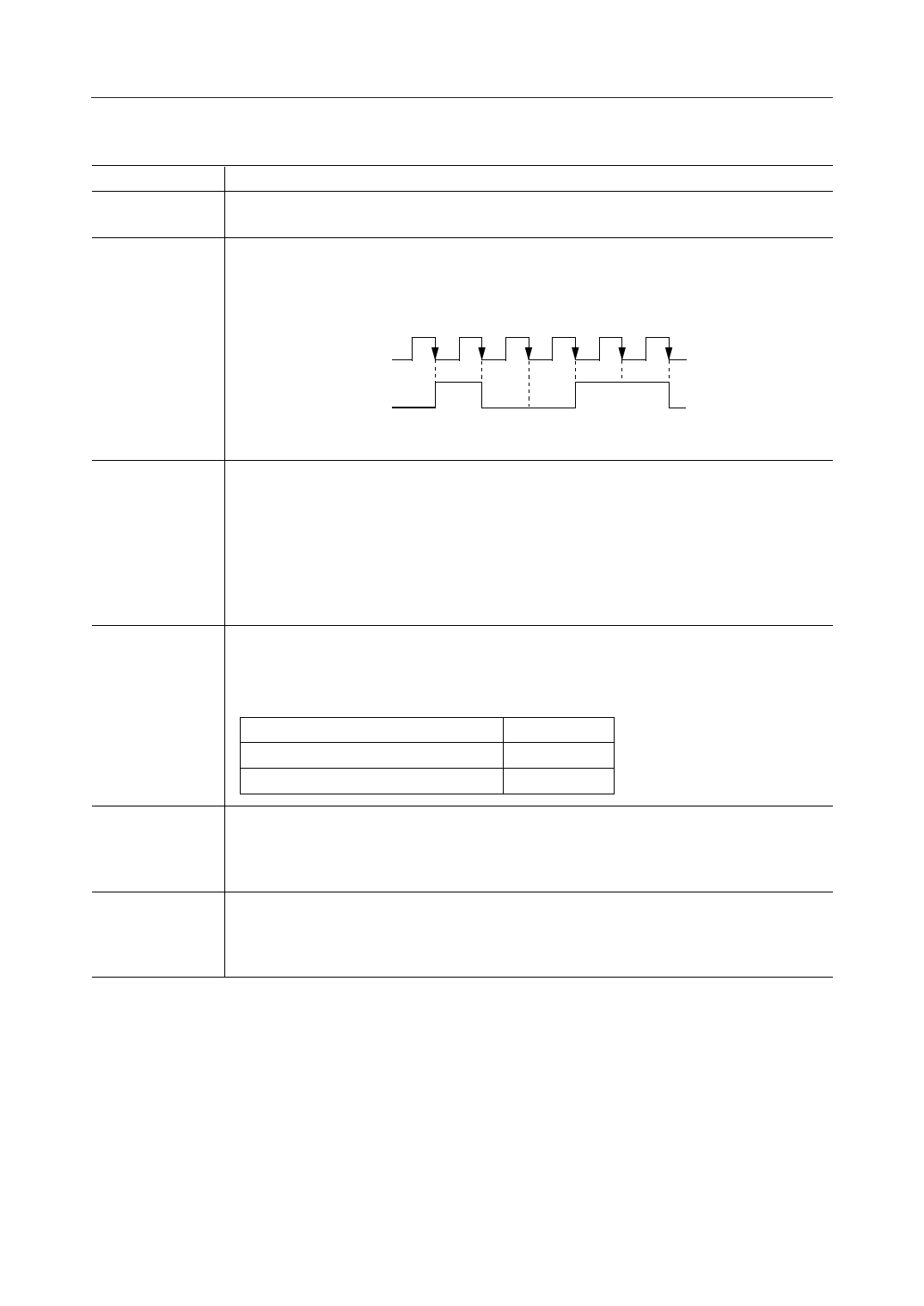
RT
RD
Delay time (RT Æ RD) < 300 ns
Receive data timing clock is re-generated by digital PLL of which phase correcting speed can
be selected with CF.
When a digital "1" is put on CF and phase difference between receive data timing and RT is
more than 22.5 degree, phase correcting speed is high. In this case, as the phase difference
enters within 22.5 degrees, that speed changes to low immediately.
When digital "0" is input to CF, phase correcting speed of PLL remains low regardless of the
phase difference.
Usually, CF is connected to digital "1".
PLL's lock-in characteristics can be selected with CT.
When digital "1" is put on CT, PLL requires max. 50-bit alternative data pattern. On the other
hand, when digital "0" is input to CT,
PLL can be locked in below 18-bit data.
Equipment
CT
Personal/MCA wireless terminals
"1"
MCA wireless bases
"0"
Control signal for the internal connection of AO.
Refer to column AO.
When digital "0" is input to this pin, transmit LPF enters in power down mode, but the output
buffer operational amplifier remains active.
+5 V power supply.
This device is sensitive to supply noises as switched capacitor techniques are utilized.
Bypass capacitors of more than 2.2 mF between VDD and AG, and between VDD and DG are
indispensable to ensure the performance.
6/13
Share Link: 