LT1671CMS8 Просмотр технического описания (PDF) - Linear Technology
Номер в каталоге
Компоненты Описание
Список матч
LT1671CMS8 Datasheet PDF : 12 Pages
| |||
LT1671
APPLICATIONS INFORMATION
5V 0.01µF*
0V
–100mV
0.1µF 130Ω
25Ω
25Ω
10k
+
Q
LT1671
–
Q
PULSE
IN
0V
2N3866
V1** 50Ω
0.01µF
–3V
50Ω
400Ω 750Ω
–5V
FET PROBE
FET PROBE
* TOTAL LEAD LENGTH INCLUDING DEVICE PIN.
SOCKET AND CAPACITOR LEADS SHOULD BE
LESS THAN 0.5 IN. USE GROUND PLANE
** (VOS + OVERDRIVE)/200
1671 F02
–5V
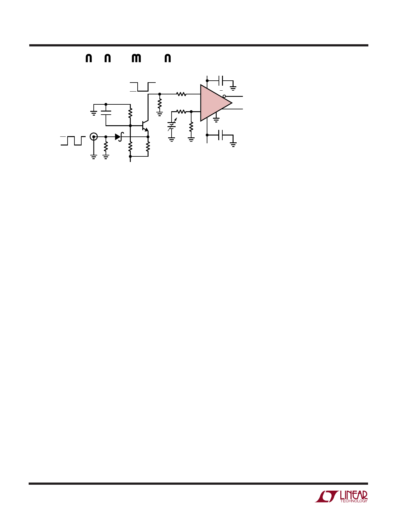
Figure 2. Response Time Test Circuit
circuit is the lack of feedthrough from the generator to the
comparator input. This prevents overshoot on the com-
parator input, which would give a false fast reading on
comparator response time.
To adjust the circuit for exactly 5mV overdrive, V1 is
adjusted so that the LT1671 output under test settles to
1.4V (in the linear region). Then V1 is changed by – 1V to
set overdrive to 5mV.
High Speed Design Techniques
A substantial amount of design effort has made the LT1671
relatively easy to use. It is much less prone to oscillation
than some slower comparators, even with slow input
signals. However, as with any high speed comparator,
there are a number of problems which may arise because
of PC board layout and design. The most common prob-
lem involves power supply bypassing. Bypassing is nec-
essary to maintain low supply impedance. DC resistance
and inductance in supply wires and PC traces can quickly
build up to unacceptable levels. This allows the supply line
to move with changing internal current levels of the
connected devices. This will almost always result in
improper operation. In addition, adjacent devices con-
nected through an unbypassed supply can interact with
each other through the finite supply impedances. Bypass
capacitors furnish a simple solution to this problem by
providing a local reservoir of energy at the device, keeping
supply impedances low.
Bypass capacitors should be as close as possible to the
LT1671. A good high frequency capacitor such as a 0.1µF
ceramic is recommended, in parallel with a larger capaci-
tor such as a 4.7µF tantalum.
Poor trace routes and high source impedances are also
common sources of problems. Be sure to keep trace
lengths as short as possible, and avoid running any output
trace adjacent to an input trace to prevent unnecessary
coupling. If output traces are longer than a few inches, be
sure to terminate them with a resistor to eliminate any
reflections that may occur. Resistor values are typically
250Ω to 400Ω. Also, be sure to keep source impedances
as low as possible, preferably 1kΩ or less.
About Level Shifts
The LT1671’s logic output will interface with many cir-
cuits directly. Many applications, however, require some
form of level shifting of the output swing. With LT1671-
based circuits this is not trivial because it is desirable to
maintain very low delay in the level shifting stage. When
designing level shifters, keep in mind that the TTL output
of the LT1671 is a sink-source pair (Figure 3) with good
ability to drive capacitance (such as feedforward capaci-
tors). Figure 4 shows a noninverting voltage gain stage
with a 15V output. When the LT1671 switches, the base-
emitter voltages at the 2N2369 reverse, causing it to
switch very quickly. The 2N3866 emitter-follower gives a
low impedance output and the Schottky diode aids cur-
rent sink capability.
8
Share Link: 