74HC4053 Просмотр технического описания (PDF) - Fairchild Semiconductor
Номер в каталоге
Компоненты Описание
Список матч
74HC4053
Fairchild Semiconductor

74HC4053 Datasheet PDF : 11 Pages
| |||
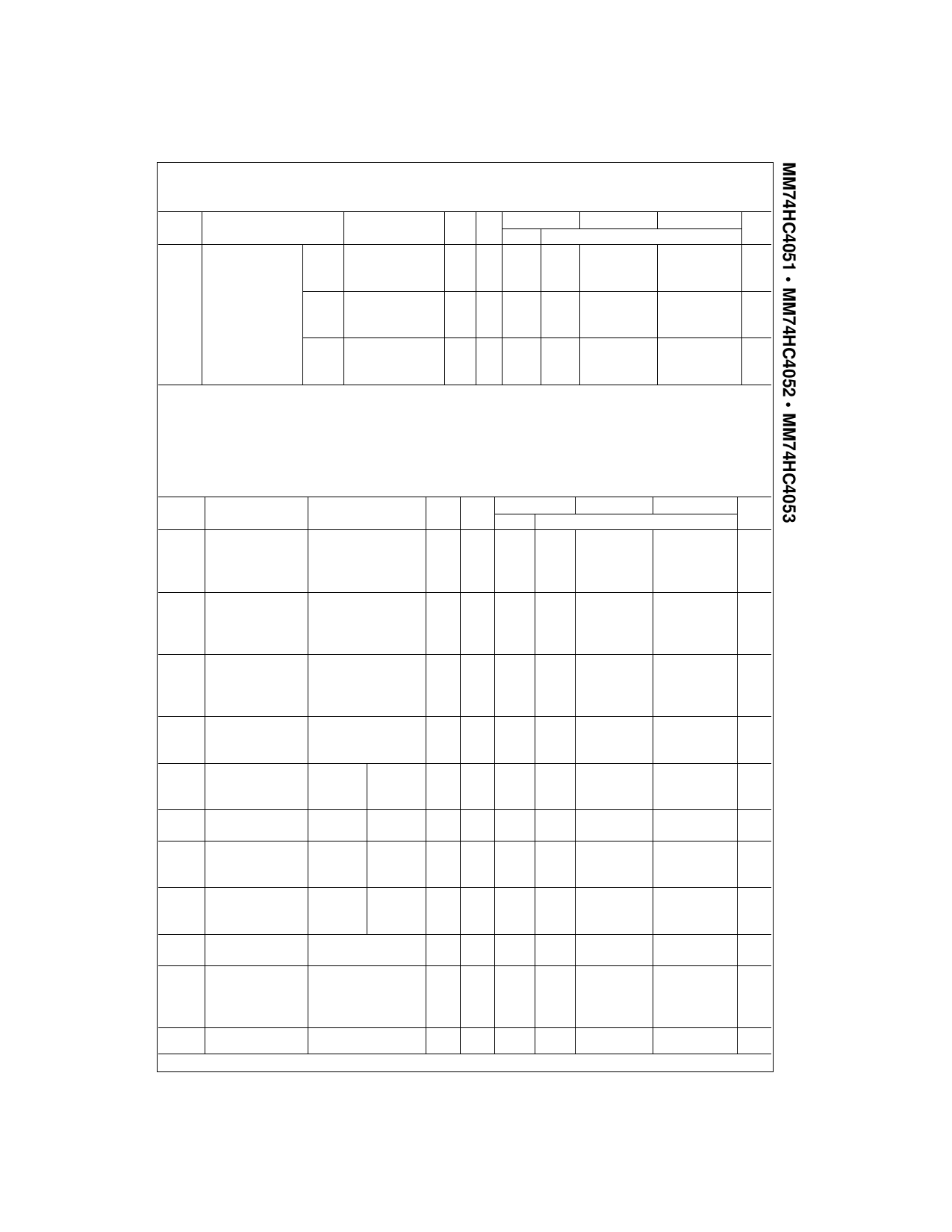
DC Electrical Characteristics (Continued)
Symbol
Parameter
Conditions
VEE VCC
TA = 25°C
Typ
TA = −40 to 85°C TA = −55 to 125°C Units
Guaranteed Limits
IIZ
Maximum Switch
VOS = VCC or VEE
GND 6.0V
±0.2
±2.0
±2.0
µA
“OFF” Leakage
HC4051 VIS = VEE or VCC
−6.0V 6.0V
±0.4
±4.0
±4.0
µA
Current (Common Pin)
VINH = VIH
VOS = VCC or VEE
GND 6.0V
±0.1
±1.0
±1.0
µA
HC4052 VIS = VEE or VCC
−6.0V 6.0V
±0.2
±2.0
±2.0
µA
VINH = VIH
VOS = VCC or VEE
GND 6.0V
±0.1
±1.0
±1.0
µA
HC4053 VIS = VEE or VCC
−6.0V 6.0V
±0.1
±1.0
±1.0
µA
VINH = VIH
Note 4: For a power supply of 5V ±10% the worst case on resistances (RON) occurs for HC at 4.5V. Thus the 4.5V values should be used when designing
with this supply. Worst case VIH and VIL occur at VCC = 5.5V and 4.5V respectively. (The VIH value at 5.5V is 3.85V.) The worst case leakage current occur
for CMOS at the higher voltage and so the 5.5V values should be used.
Note 5: At supply voltages (VCC–VEE) approaching 2V the analog switch on resistance becomes extremely non-linear. Therefore it is recommended that
these devices be used to transmit digital only when using these supply voltages.
AC Electrical Characteristics
VCC = 2.0V−6.0V, VEE = 0V−6V, CL = 50 pF (unless otherwise specified)
Symbol
Parameter
Conditions
VEE VCC
tPHL, tPLH Maximum Propagation
Delay Switch In to Out
tPZL, tPZH Maximum Switch Turn RL = 1 kΩ
“ON” Delay
tPHZ, tPLZ Maximum Switch Turn
“OFF” Delay
fMAX
THD
CIN
CIN
CIN
Minimum Switch
Frequency Response
20 log (VI/VO) = 3 dB
Control to Switch
Feedthrough Noise
Crosstalk between
any Two Switches
Switch OFF Signal
Feedthrough
Isolation
Sinewave Harmonic
Distortion
RL = 600Ω,
f = 1 MHz,
CL = 50 pF
RL = 600Ω,
f = 1 MHz
RL = 600Ω,
f = 1 MHz,
VCTL = VIL
RL = 10 kΩ,
CL = 50 pF,
f = 1 kHz
VIS = 4 VPP
VIS = 8 VPP
VIS = 4 VPP
VIS = 8 VPP
VIS = 4 VPP
VIS = 8 VPP
VIS = 4 VPP
VIS = 8 VPP
Maximum Control
Input Capacitance
Maximum Switch
Input
Input Capacitance
4051 Common
4052 Common
4053 Common
Maximum Feedthrough
Capacitance
GND
GND
−4.5V
−6.0V
GND
GND
−4.5V
−6.0V
GND
GND
−4.5V
−6.0V
GND
−4.5V
0V
−4.5V
0V
−4.5V
0V
−4.5V
0V
−4.5V
2.0V
4.5V
4.5V
6.0V
2.0V
4.5V
4.5V
6.0V
2.0V
4.5V
4.5V
6.0V
4.5V
4.5V
4.5V
4.5V
4.5
4.5V
4.5V
4.5V
4.5V
4.5V
TA = 25°C
Typ
25
60
5
12
4
8
3
7
92
355
69
16
46
15
41
65
290
28
58
18
37
16
32
30
35
1080
250
−52
−50
−42
−44
0.013
0.008
5
10
15
90
45
30
5
TA = −40 to 85°C TA = −55 to 125°C Units
Guaranteed Limits
75
90
ns
15
18
ns
12
14
ns
11
13
ns
435
515
ns
87
103
ns
58
69
ns
51
62
ns
365
435
ns
73
87
ns
46
56
ns
41
48
ns
MHz
MHz
mV
mV
dB
dB
dB
dB
%
%
10
10
pF
pF
pF
5
www.fairchildsemi.com
Share Link: