ML6698 Просмотр технического описания (PDF) - Micro Linear Corporation
Номер в каталоге
Компоненты Описание
Список матч
ML6698 Datasheet PDF : 12 Pages
| |||
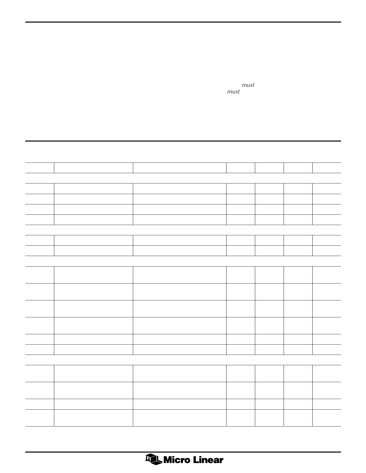
ABSOLUTE MAXIMUM RATINGS
Absolute maximum ratings are those values beyond which
the device could be permanently damaged. Absolute
maximum ratings are stress ratings only and functional
device operation is not implied.
VCC Supply Voltage Range ................... GND –0.3V to 6V
Input Voltage Range
Digital Inputs ....................... GND –0.3V to VCC + 0.3V
TPINP, TPINN, 10BTTXINP,
10BTTXINN ..................... GND –0.3V to VCC + 0.3V
Output Current
TPOUTP, TPOUTN .............................................. 60mA
All other outputs .................................................. 10mA
ML6698
Junction Temperature ............................................. 150°C
Storage Temperature .............................. .. –65°C to 150°C
Lead Temperature (Soldering, 10 sec) ..................... 260°C
OPERATING CONDITIONS
VCC Supply Voltage ............................................ 5V ± 5%
All VCC supply pins must be within 0.1V of each other.
All GND pins must be within 0.1V of each other.
TA, Ambient temperature ................................ 0°C to 70°C
RGMSET ..................................................... 9.53ký ± 1%
RTSET .......................................................... 2.49ký ± 1%
Receive transformer insertion loss ........................ <–0.5dB
DC ELECTRICAL CHARACTERISTICS
Over full range of operating conditions unless otherwise specified (Note 1)
SYMBOL
PARAMETER
CONDITIONS
TTL Inputs (TSM<4:0>, TXC, SEL100/10, PWRDN, LPBK)
VIL
Input Low Voltage
VIH
Input High Voltage
IIL
Input Low Current
IIH
Input High Current
TTL Outputs (RSM<4:0>, RXC, SDO)
IIL = –400µA
IIH = 100µA
VIN = 0.4V
VIN = 2.7V
VOL
VOH
Receiver
Output Low Voltage
Output High Voltage
IOL = 4mA
IOH = –4mA
VICM
TPINP/N Input Common-Mode 100ý Termination across TPINP/N
Voltage
VID
TPINP-TPINN Differential Input
Voltage Range
RIDR
TPINP-TPINN Differential
Input Resistance
IICM
TPINP/N Common-Mode Input
Current
IRGM
RGMSET Input Current
IRT
RTSET Input Current
Transmitter
RGMSET = 9.53ký
RTSET = 2.49ký
ITD100
TPOUTP/N 100BASE-TX Mode Note 2, 3
Differential Output Current
ITD10
TPOUTP/N 10BASE-T
Mode Differential Output Current
ITOFF
ITXI
TPOUTP/N Off-State Output
TPOUTP/N Differential Output
Current Imbalance
RL = 200, 1%
RL = 200, 1%
MIN
TYP
MAX
UNITS
2.0
–200
0.8
V
V
µA
100
µA
0.4
V
2.4
V
VCC – 1.26
V
–3.0
3.0
V
10.0k
ý
+10
µA
130
µA
500
µA
±19
±21
mA
±55
±60
±65
mA
0
1.5
mA
500
µA
5
Share Link: 