MIC5219 Просмотр технического описания (PDF) - Micrel
Номер в каталоге
Компоненты Описание
Список матч
MIC5219 Datasheet PDF : 14 Pages
| |||
Micrel, Inc.
PD × 50mA = 0.875 × 173mW
PD × 50mA = 151mW
The power dissipation at 500mA must also be calculated.
PD × 500mA = (5V – 3.3V) 500mA + 5V × 20mA
PD × 500mA = 950mW
This number must be multiplied by the duty cycle at which it
would be operating, 12.5%.
PD × = 0.125 × 950mW
PD × = 119mW
The total power dissipation of the device under these condi-
tions is the sum of the two power dissipation figures.
PD(total) = PD × 50mA + PD × 500mA
PD(total) = 151mW + 119mW
PD(total) = 270mW
The total power dissipation of the regulator is less than the
maximum power dissipation of the SOT-23-5 package at room
temperature, on a minimum footprint board and therefore
would operate properly.
Multilayer boards with a ground plane, wide traces near the
pads, and large supply-bus lines will have better thermal
conductivity.
For additional heat sink characteristics, please refer to Mi-
crel “Application Hint 17, Designing P.C. Board Heat Sinks”,
included in Micrel’s Databook. For a full discussion of heat
sinking and thermal effects on voltage regulators, refer to
“Regulator Thermals” section of Micrel’s Designing with Low-
Dropout Voltage Regulators handbook.
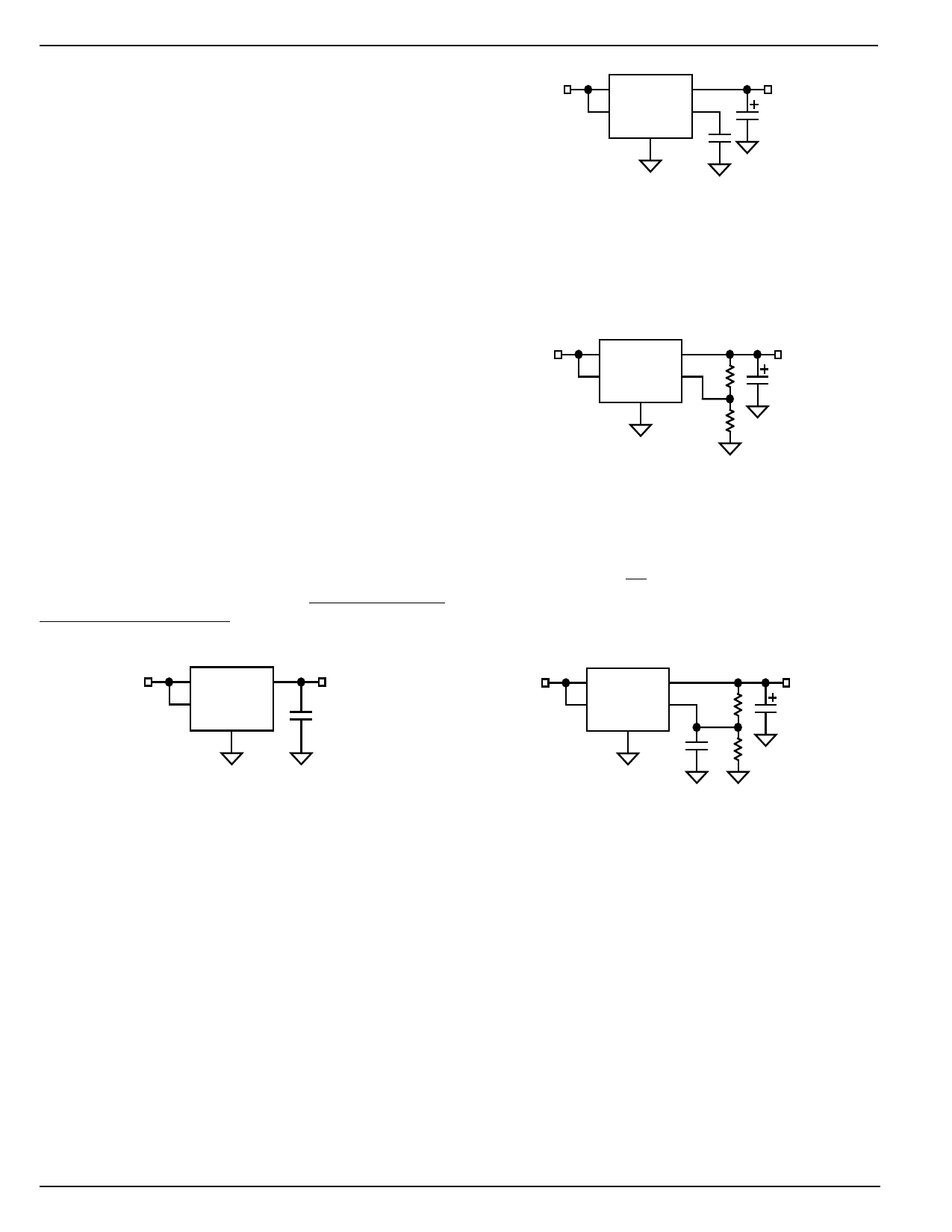
Fixed Regulator Circuits
VIN
MIC5219-x.x
IN OUT
VO U T
EN BYP
GND
1µF
Figure 5. Low-Noise Fixed Voltage Regulator
Figure 5 shows a basic MIC5219‑x.xBMX fixed-voltage regu-
lator circuit. A 1µF minimum output capacitor is required for
basic fixed-voltage applications.
MIC5219
VIN
MIC5219-x.x
IN OUT
VO U T
EN BYP
GND
2.2µF
470pF
Figure 6. Ultra-Low-Noise Fixed Voltage Regulator
Figure 6 includes the optional 470pF noise bypass capacitor
between BYP and GND to reduce output noise. Note that the
minimum value of COUT must be increased when the bypass
capacitor is used.
Adjustable Regulator Circuits
VIN
MIC5219
IN OUT
VO U T
EN ADJ R1
GND
1µF
R2
Figure 7. Low-Noise Adjustable Voltage Regulator
Figure 7 shows the basic circuit for the MIC5219 adjustable
regulator. The output voltage is configured by selecting values
for R1 and R2 using the following formula:
VOUT
= 1.242V
R2
R1
+ 1
Although ADJ is a high-impedance input, for best performance,
R2 should not exceed 470kΩ.
VIN
MIC5219
IN OUT
VO U T
EN ADJ
GND
R1
2.2µF
R2
470pF
Figure 8. Ultra-Low-Noise Adjustable Application
Figure 8 includes the optional 470pF bypass capacitor from
ADJ to GND to reduce output noise.
June 2009
12
M0371-061809
Share Link: 