MCM69P736ZP4 Просмотр технического описания (PDF) - Motorola => Freescale
Номер в каталоге
Компоненты Описание
Список матч
MCM69P736ZP4 Datasheet PDF : 16 Pages
| |||
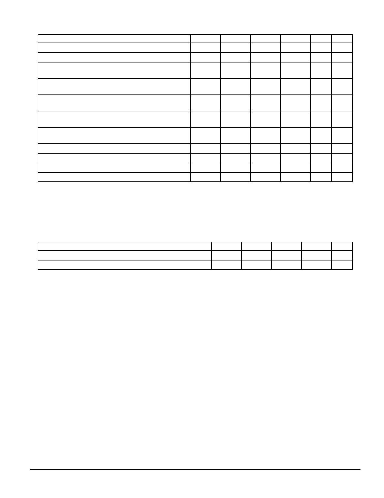
DC CHARACTERISTICS AND SUPPLY CURRENTS
Parameter
Symbol
Min
Typ
Max
Unit Notes
Input Leakage Current (0 V ≤ Vin ≤ VDD)
Ilkg(I)
—
—
±1
µA
Output Leakage Current (0 V ≤ Vin ≤ VDDQ)
Ilkg(O)
—
—
±1
µA
AC Supply Current (Device Selected, All Outputs Open,
Freq = Max) Includes VDD Only
IDDA
—
—
375
mA 1, 2, 3
CMOS Standby Supply Current (Device Deselected, Freq = 0,
ISB2
—
—
45
mA
4, 5
VDD = Max, All Inputs Static at CMOS Levels)
TTL Standby Supply Current (Device Deselected, Freq = 0,
VDD = Max, All Inputs Static at TTL Levels)
ISB3
—
—
50
mA
4, 6
Clock Running (Device Deselected, Freq = Max, VDD = Max,
All Inputs Toggling at CMOS Levels)
ISB4
—
—
165
mA
4, 5
Static Clock Running (Device Deselected, Freq = Max,
VDD = Max, All Inputs Static at TTL Levels)
ISB5
—
—
95
mA
4, 6
Output Low Voltage (IOL = 2 mA) VDDQ = 2.5 V
VOL
—
—
0.7
V
Output High Voltage (IOL = – 2 mA) VDDQ = 2.5 V
VOH
1.7
—
—
V
Output Low Voltage (IOL = 8 mA) VDDQ = 3.3 V
VOL2
—
—
0.4
V
Output High Voltage (IOL = – 4 mA) VDDQ = 3.3 V
VOH2
2.4
—
—
V
NOTES:
1. Reference AC Operating Conditions and Characteristics for input and timing.
2. All addresses transition simultaneously low (LSB) then high (MSB).
3. Data states are all zero.
4. Device is deselected as defined by the Truth Table.
5. CMOS levels for I/O’s are VIT ≤ VSS + 0.2 V or ≥ VDDQ – 0.2 V. CMOS levels for other inputs are Vin ≤ VSS + 0.2 V or ≥ VDD – 0.2 V.
6. TTL levels for I/O’s are VIT ≤ VIL or ≥ VIH2. TTL levels for other inputs are Vin ≤ VIL or ≥ VIH.
CAPACITANCE (f = 1.0 MHz, dV = 3.0 V, TA = 0 to 70°C, Periodically Sampled Rather Than 100% Tested)
Parameter
Symbol
Min
Typ
Input Capacitance
Cin
—
4
Input/Output Capacitance
CI/O
—
7
Max
Unit
5
pF
8
pF
MCM69P736
8
MOTOROLA FAST SRAM
Share Link: 