MCM63P636ZP200 Просмотр технического описания (PDF) - Motorola => Freescale
Номер в каталоге
Компоненты Описание
Список матч
MCM63P636ZP200 Datasheet PDF : 27 Pages
| |||
CAPACITANCE AND INDUCTANCE (See Notes 1, 2, and 3)
TQFP
Capacitance (pF)
Inductance (nH)
Pin Description
Min
Max
Min
Max
I/O Pins
5
7
2
10
Data Strobe Pins
5
7
2
10
Input Pins
3
5
2
10
ADS Pin
5
7
2
10
K and SK Pins
3.5
4.5
2
10
TCK Boundary Scan Pin
—
—
—
—
Boundary Scan Input Pins
—
—
—
—
TDO Boundary Scan Pin
—
—
—
—
NOTES:
1. Parameters are periodically sampled rather than 100% tested.
2. Capacitance variation part to part on the same pin is ± 0.25 pF.
3. Inductance variation part to part on the same pin is ± 1 nH.
PBGA
Capacitance (pF)
Inductance (nH)
Min
Max
Min
Max
5.5
7.5
2.5
4.5
5.5
7.5
2.5
4.5
3.5
5.5
2.5
4
5.5
7.5
2.5
4.5
4
5
1.5
3
—
5
—
—
—
8
—
—
—
8
—
—
AC OPERATING CONDITIONS AND CHARACTERISTICS
(VDD = 3.3 V ± 200 mV, Unless Otherwise Noted)
AC TEST CONDITIONS
Parameter
Value
Unit
Input Timing Reference Level
Input Pulse Levels
VDDQ/2
V
0 to 2.0
V
Input Rise/Fall Time (20 to 80%)
1
V/ns
Output Timing Reference Level
Die Temperature
VDDQ/2
V
TJ–250
115
°C
TJ–225
115
TJ–200
115
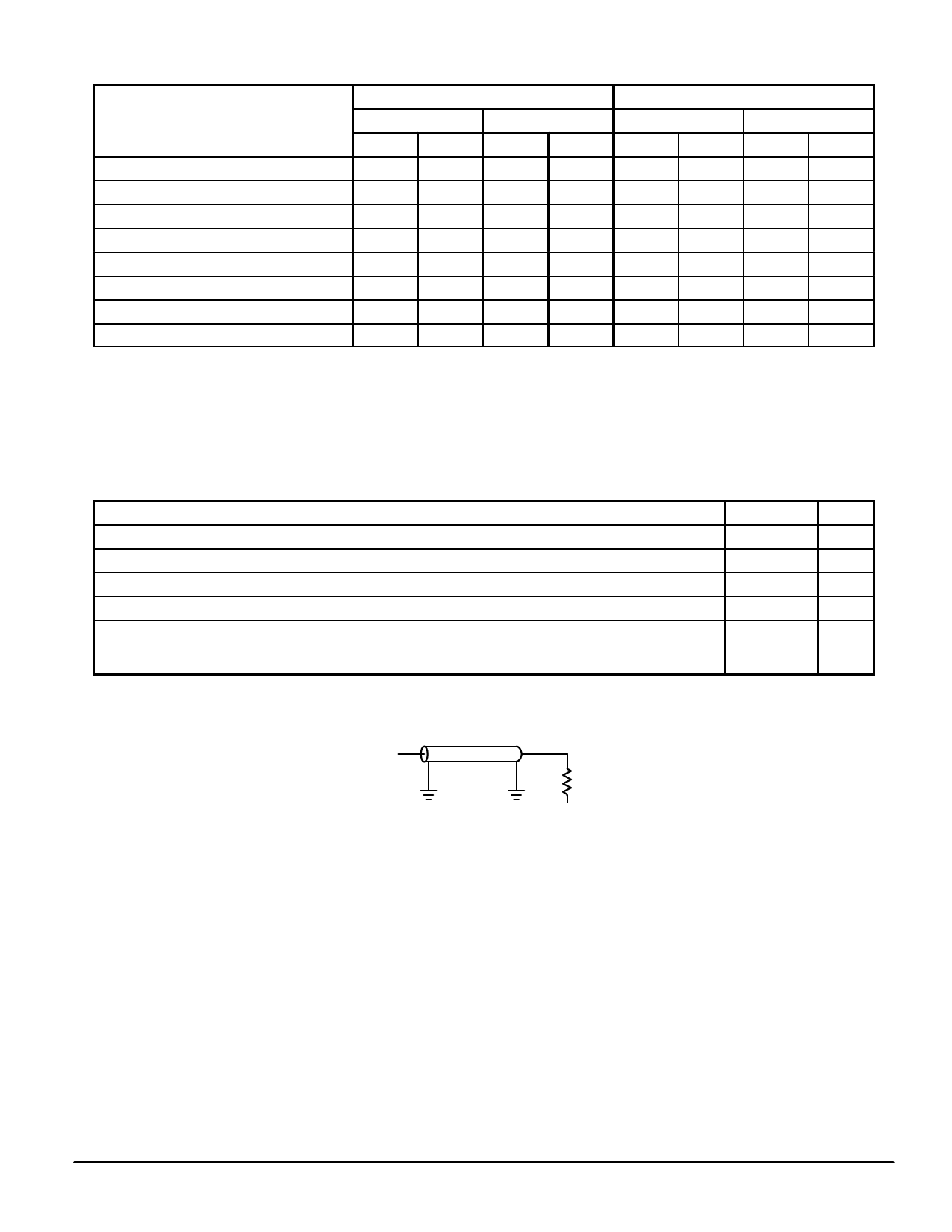
OUTPUT
Z0 = 50 Ω
RL
1.0 V
Figure 4. AC Output Test Load
(TBD)
Figure 5. Lumped Capacitive Load and Typical Derating Curve
MCM63P636
10
MOTOROLA FAST SRAM
Share Link: 