MC74HC393J Просмотр технического описания (PDF) - ON Semiconductor
Номер в каталоге
Компоненты Описание
Список матч
MC74HC393J Datasheet PDF : 7 Pages
| |||
MC74HC393
PIN DESCRIPTIONS
INPUTS
Clock (Pins 1, 13)
Clock input. The internal flip−flops are toggled and the
counter state advances on high−to−low transitions of the
clock input.
CONTROL INPUTS
Reset (Pins 2, 12)
Active−high, asynchronous reset. A separate reset is
provided for each counter. A high at the Reset input
prevents counting and forces all four outputs low.
OUTPUTS
Q1, Q2, Q3, Q4 (Pins 3, 4, 5, 6, 8, 9, 10, 11)
Parallel binary outputs Q4 is the most significant bit.
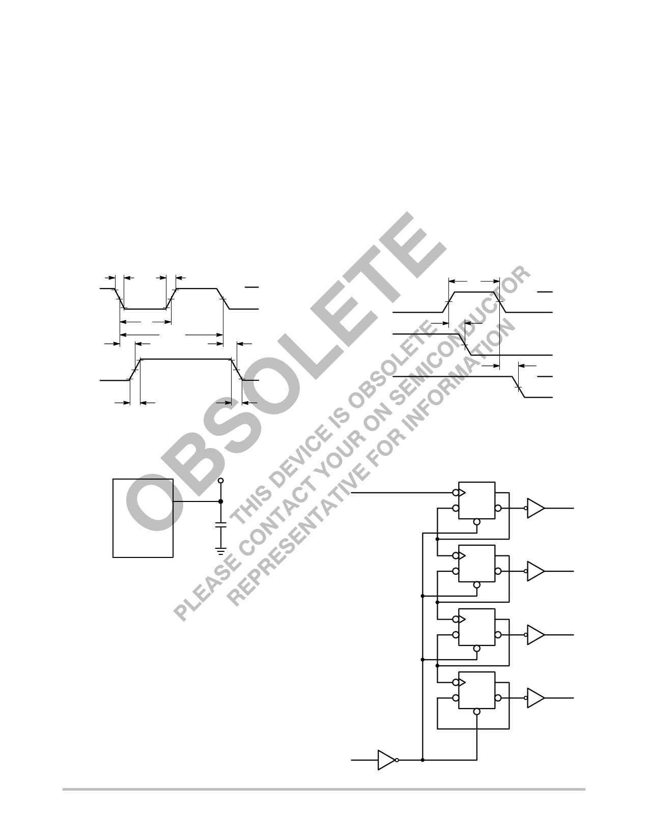
SWITCHING WAVEFORMS
tf
tr
90%
VCC
CLOCK
50%
10%
GND
tw
1/fmax
tPLH
tPHL
90%
Q 50%
10%
tTLH
tTHL
Figure 1.
tw
RESET
50%
VCC
GND
tPHL
Q
CLOCK
50%
trec
VCC
50%
GND
Figure 2.
DEVICE
UNDER
TEST
TEST
POINT
OUTPUT
CL*
*Includes all probe and jig capacitance
Figure 3. Test Circuit
CLOCK 1, 13
EXPANDED LOGIC DIAGRAM
CQ
DQ
3, 11 Q1
CQ
DQ
4, 10 Q2
CQ
DQ
5, 9 Q3
CQ
DQ
6, 8 Q4
RESET 2, 12
http://onsemi.com
4
Share Link: 