MC74HC132ADTR2 Просмотр технического описания (PDF) - ON Semiconductor
Номер в каталоге
Компоненты Описание
Список матч
MC74HC132ADTR2 Datasheet PDF : 10 Pages
| |||
MC74HC132A
AC ELECTRICAL CHARACTERISTICS (CL = 50 pF, Input tr = tf = 6.0 ns)
VCC
Guaranteed Limit
Symbol
Parameter
ÎÎÎÎÎÎÎÎÎÎÎÎÎÎÎÎÎÎÎÎÎÎÎÎÎÎÎÎÎÎÎÎÎ tPLH,
ÎÎÎÎÎÎÎÎÎÎÎÎÎÎÎÎÎÎÎÎÎÎÎÎÎÎÎÎÎÎÎÎÎ tPHL
Maximum Propagation Delay, Input A or B to Output Y
(Figures 3 and 4)
ÎÎÎÎÎÎÎÎÎÎÎÎÎÎÎÎÎÎÎÎÎÎÎÎÎÎÎÎÎÎÎÎÎ tTLH,
ÎÎÎÎÎÎÎÎÎÎÎÎÎÎÎÎÎÎÎÎÎÎÎÎÎÎÎÎÎÎÎÎÎ tTHL
Maximum Output Transition Time, Any Output
(Figures 3 and 4)
ÎÎÎÎÎÎÎÎÎÎÎÎÎÎÎÎÎÎÎÎÎÎÎÎÎÎÎÎÎÎÎÎÎÎÎÎÎÎÎÎÎÎÎÎÎÎÎÎÎÎÎÎÎÎÎÎÎÎÎÎÎÎÎÎÎÎ Cin Maximum Input Capacitance
V *55_C to 25_C v85_C v125_C Unit
2.0
125
4.5
25
6.0
21
155
190
ns
31
38
26
32
2.0
75
4.5
15
6.0
13
95
110
ns
19
22
16
19
—
10
10
10
pF
10. For propagation delays with loads other than 50 pF, and information on typical parametric values, see the ON Semiconductor High−Speed
CMOS Data Book (DL129/D).
Typical @ 25°C, VCC = 5.0 V
CPD Power Dissipation Capacitance (per Gate) (Note 11)
24
pF
11. Used to determine the no−load dynamic power consumption: PD = CPD VCC2f + ICC VCC. For load considerations, see the ON
Semiconductor High−Speed CMOS Data Book (DL129/D).
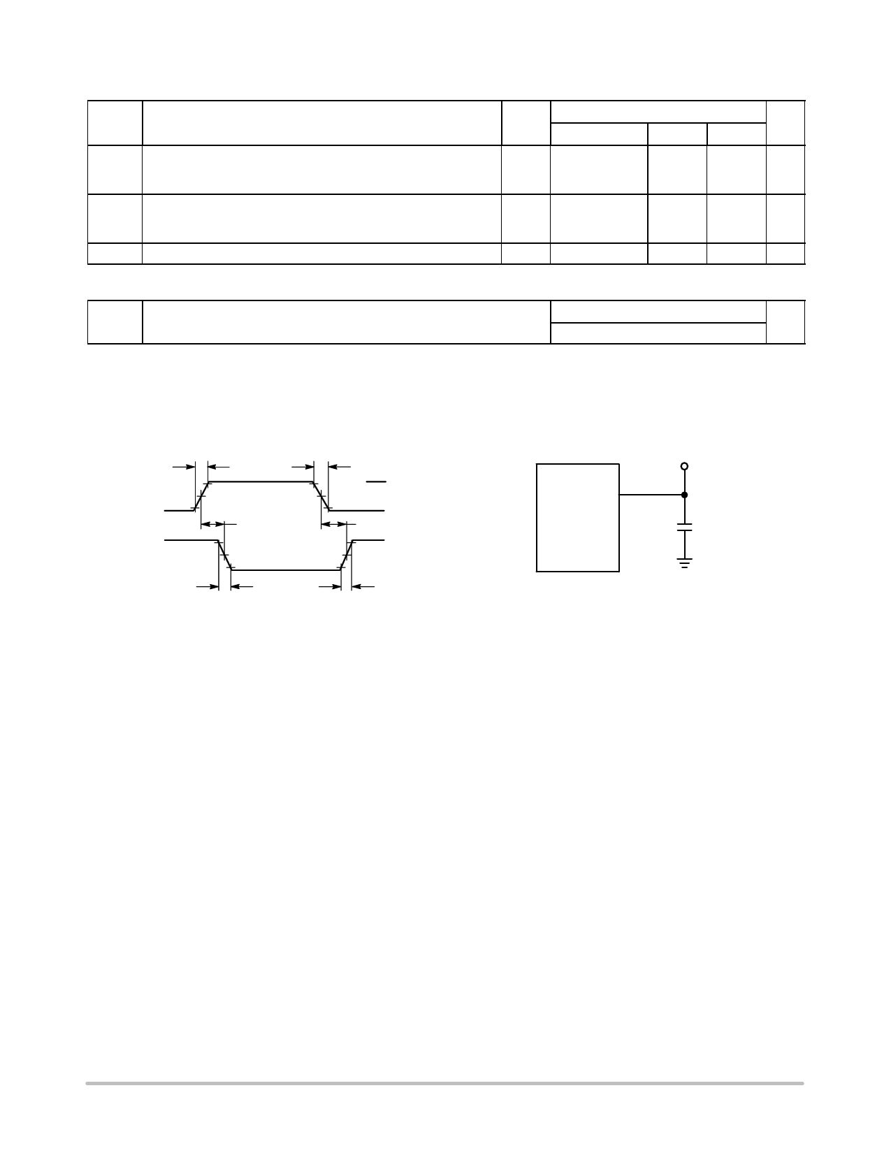
INPUT
A OR B
Y
tr
90%
50%
10%
tPHL
90%
50%
10%
tTHL
tf
VCC
GND
tPLH
tTLH
Figure 3. Switching Waveforms
DEVICE
UNDER
TEST
TEST POINT
OUTPUT
CL*
*Includes all probe and jig capacitance
Figure 4. Test Circuit
http://onsemi.com
5
Share Link: 