MC14511B Просмотр технического описания (PDF) - ON Semiconductor
Номер в каталоге
Компоненты Описание
Список матч
MC14511B Datasheet PDF : 10 Pages
| |||
MC14511B
This device contains protection circuitry to protect the inputs against damage due to high static voltages or electric fields.
However, it is advised that normal precautions be taken to avoid application of any voltage higher than maximum rated voltages
to this high−impedance circuit. A destructive high current mode may occur if Vin and Vout are not constrained to the range
VSS v (Vin or Vout) v VDD.
Due to the sourcing capability of this circuit, damage can occur to the device if VDD is applied, and the outputs are shorted
to VSS and are at a logical 1 (See Maximum Ratings).
Unused inputs must always be tied to an appropriate logic voltage level (e.g., either VSS or VDD).
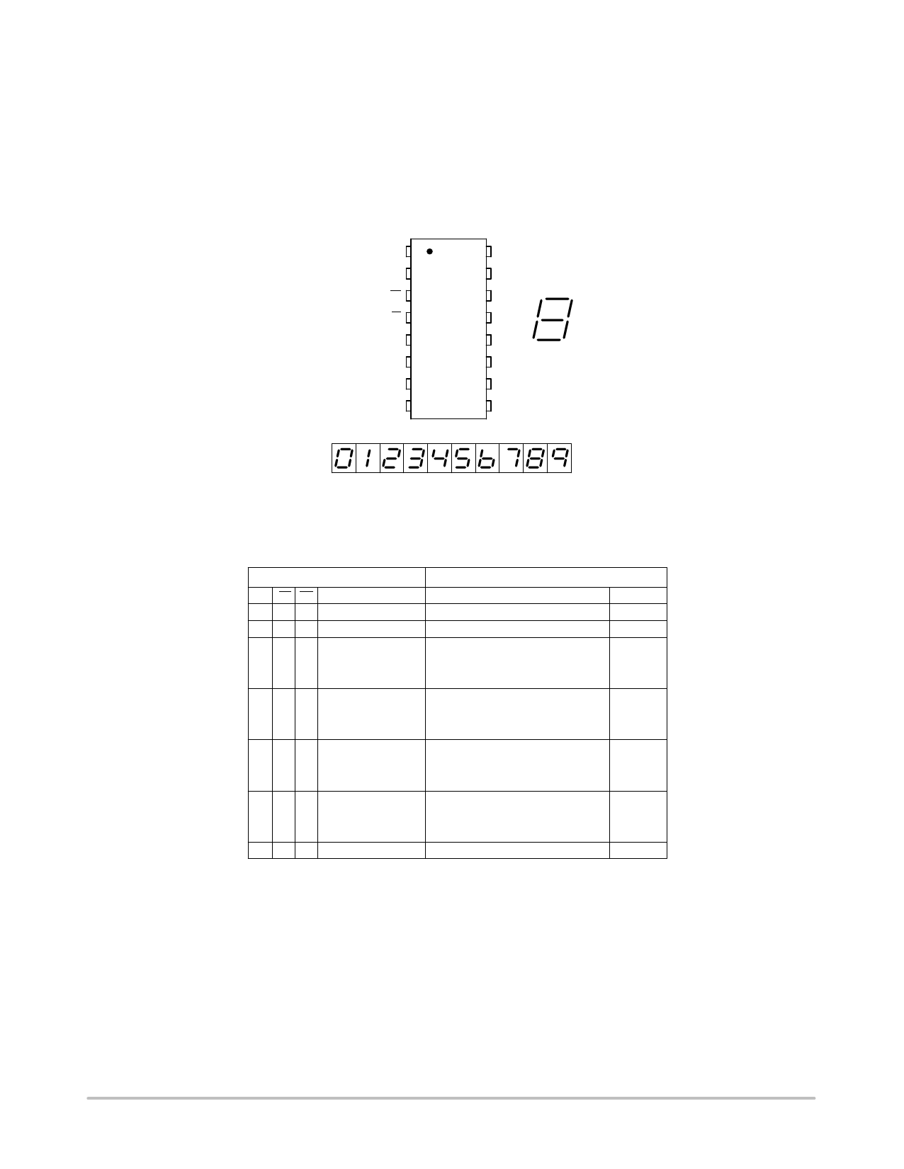
PIN ASSIGNMENT
B1
C2
LT 3
BI 4
LE 5
D6
16 VDD
15 f
14 g
13 a
12 b
11 c
a
f gb
e
c
d
A7
10 d
VSS 8
9e
DISPLAY
012 345 6789
TRUTH TABLE
Inputs
Outputs
LE BI LT D C B A a b c d e f g Display
X X0 X X X X 1 1 1 1 1 1 1
8
X 0 1 X X X X 0 0 0 0 0 0 0 Blank
0 11 0 0 0 0 1 1 1 1 1 1 0
0
0 11 0 0 0 1 0 1 1 0 0 0 0
1
0 11 0 0 1 0 1 1 0 1 1 0 1
2
0 11 0 0 1 1 1 1 1 1 0 0 1
3
0 11 0 1 0 0 0 1 1 0 0 1 1
4
0 11 0 1 0 1 1 0 1 1 0 1 1
5
0 11 0 1 1 0 0 0 1 1 1 1 1
6
0 11 0 1 1 1 1 1 1 0 0 0 0
7
0 11 1 0 0 0 1 1 1 1 1 1 1
8
0 11 1 0 0 1 1 1 1 0 0 1 1
9
0 1 1 1 0 1 0 0 0 0 0 0 0 0 Blank
0 1 1 1 0 1 1 0 0 0 0 0 0 0 Blank
0 1 1 1 1 0 0 0 0 0 0 0 0 0 Blank
0 1 1 1 1 0 1 0 0 0 0 0 0 0 Blank
0 1 1 1 1 1 0 0 0 0 0 0 0 0 Blank
0 1 1 1 1 1 1 0 0 0 0 0 0 0 Blank
1 11 X X X X
*
*
X = Don’t Care
* Depends upon the BCD code previously applied when LE = 0
http://onsemi.com
2
Share Link: 