MC14076B(2000) Просмотр технического описания (PDF) - ON Semiconductor
Номер в каталоге
Компоненты Описание
Список матч
MC14076B Datasheet PDF : 8 Pages
| |||
MC14076B
4-Bit D-Type Register
with Three-State Outputs
The MC14076B 4–Bit Register consists of four D–type flip–flops
operating synchronously from a common clock. OR gated
output–disable inputs force the outputs into a high–impedance state
for use in bus organized systems. OR gated data–disable inputs cause
the Q outputs to be fed back to the D inputs of the flip–flops. Thus they
are inhibited from changing state while the clocking process remains
undisturbed. An asynchronous master root is provided to clear all four
flip–flops simultaneously independent of the clock or disable inputs.
• Three–State Outputs with Gated Control Lines
• Fully Independent Clock Allows Unrestricted Operation for the Two
Modes: Parallel Load and Do Nothing
• Asynchronous Master Reset
• Four Bus Buffer Registers
• Supply Voltage Range = 3.0 Vdc to 18 Vdc
• Capable of Driving Two Low–Power TTL Loads or One Low–Power
Schottky TTL Load Over the Rated Temperature Range
MAXIMUM RATINGS (Voltages Referenced to VSS) (Note 1.)
Symbol
Parameter
Value
Unit
VDD
DC Supply Voltage Range
– 0.5 to +18.0
V
Vin, Vout Input or Output Voltage Range – 0.5 to VDD + 0.5
V
(DC or Transient)
Iin, Iout
Input or Output Current
(DC or Transient) per Pin
± 10
mA
PD
Power Dissipation,
per Package (Note 2.)
500
mW
TA
Ambient Temperature Range
Tstg
Storage Temperature Range
TL
Lead Temperature
(8–Second Soldering)
– 55 to +125
°C
– 65 to +150
°C
260
°C
1. Maximum Ratings are those values beyond which damage to the device
may occur.
2. Temperature Derating:
Plastic “P and D/DW” Packages: – 7.0 mW/_C From 65_C To 125_C
This device contains protection circuitry to guard against damage due to high
static voltages or electric fields. However, precautions must be taken to avoid
applications of any voltage higher than maximum rated voltages to this
v v high–impedance circuit. For proper operation, Vin and Vout should be constrained
to the range VSS (Vin or Vout) VDD.
Unused inputs must always be tied to an appropriate logic voltage level (e.g.,
either VSS or VDD). Unused outputs must be left open.
http://onsemi.com
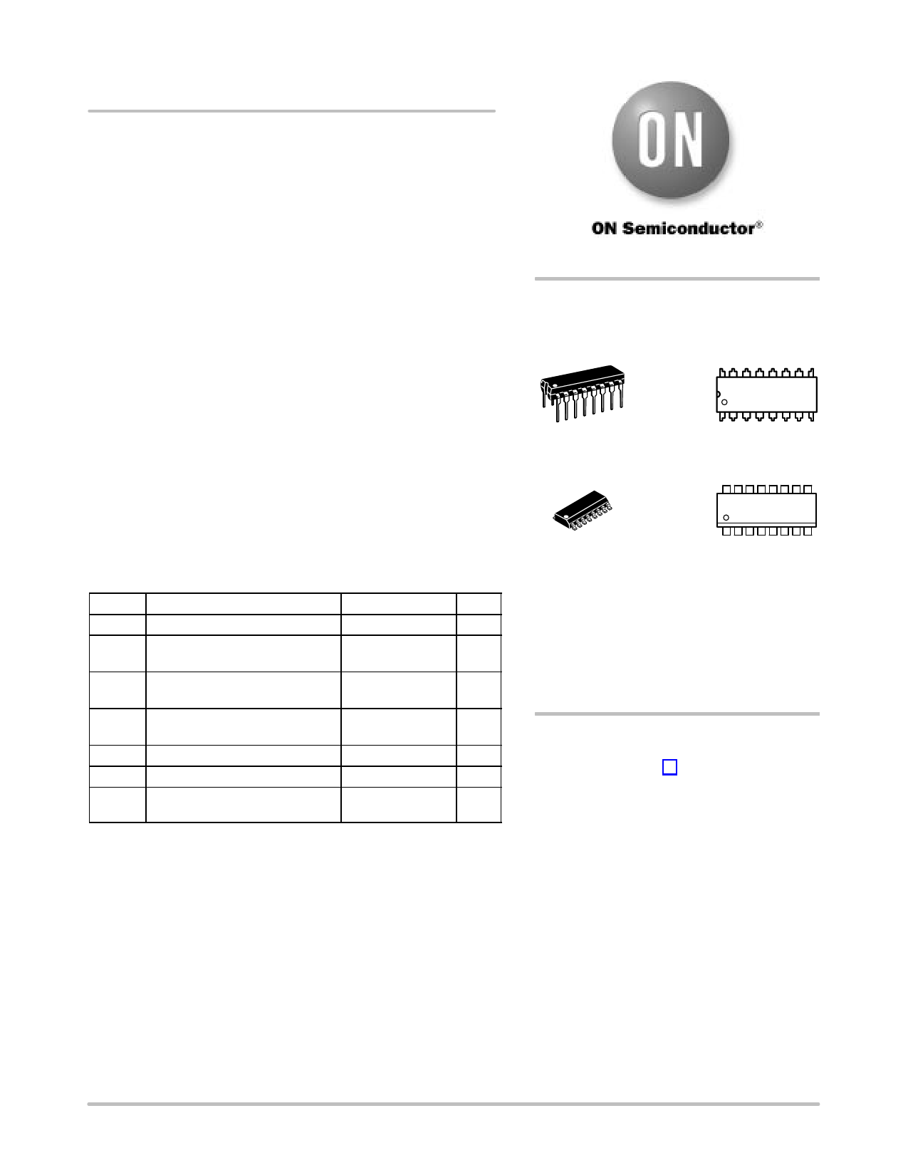
PDIP–16
P SUFFIX
CASE 648
MARKING
DIAGRAMS
16
MC14076BCP
AWLYYWW
1
SOIC–16
D SUFFIX
CASE 751B
16
14076B
AWLYWW
1
A
= Assembly Location
WL or L = Wafer Lot
YY or Y = Year
WW or W = Work Week
ORDERING INFORMATION
Device
Package
Shipping
MC14076BCP
PDIP–16
2000/Box
MC14076BD
SOIC–16
2400/Box
MC14076BDR2 SOIC–16 2500/Tape & Reel
© Semiconductor Components Industries, LLC, 2000
1
March, 2000 – Rev. 3
Publication Order Number:
MC14076B/D
Share Link: 