MBM29DL321BE Просмотр технического описания (PDF) - Fujitsu
Номер в каталоге
Компоненты Описание
Список матч
MBM29DL321BE Datasheet PDF : 80 Pages
| |||
FUJITSU SEMICONDUCTOR
DATA SHEET
DS05-20881-3E
FLASH MEMORY
CMOS
32M (4M × 8/2M × 16) BIT Dual Operation
MBM29DL32XTE/BE -80/90/12
s DESCRIPTION
The MBM29DL32XTE/BE are a 32M-bit, 3.0 V-only Flash memory organized as 4M bytes of 8 bits each or 2M
words of 16 bits each. These devices are designed to be programmed in-system with the standard system 3.0 V
VCC supply. 12.0 V VPP and 5.0 V VCC are not required for write or erase operations. The devices can also be
reprogrammed in standard EPROM programmers.
MBM29DL32XTE/BE are organized into two banks, Bank 1 and Bank 2, which can be considered to be two
separate memory arrays as far as certain operations are concerned. These devices are the same as Fujitsu’s
standard 3 V only Flash memories with the additional capability of allowing a normal non-delayed read access
from a non-busy bank of the array while an embedded write (either a program or an erase) operation is
simultaneously taking place on the other bank.
s PRODUCT LINE UP
(Continued)
Part No.
Ordering Part No.
VCC = 3.3 V
+0.3 V
–0.3 V
VCC = 3.0 V
+0.6 V
–0.3 V
Max. Address Access Time (ns)
Max. CE Access Time (ns)
Max. OE Access Time (ns)
MBM29DL32XTE/BE
80
—
—
—
90
12
80
90
120
80
90
120
30
35
50
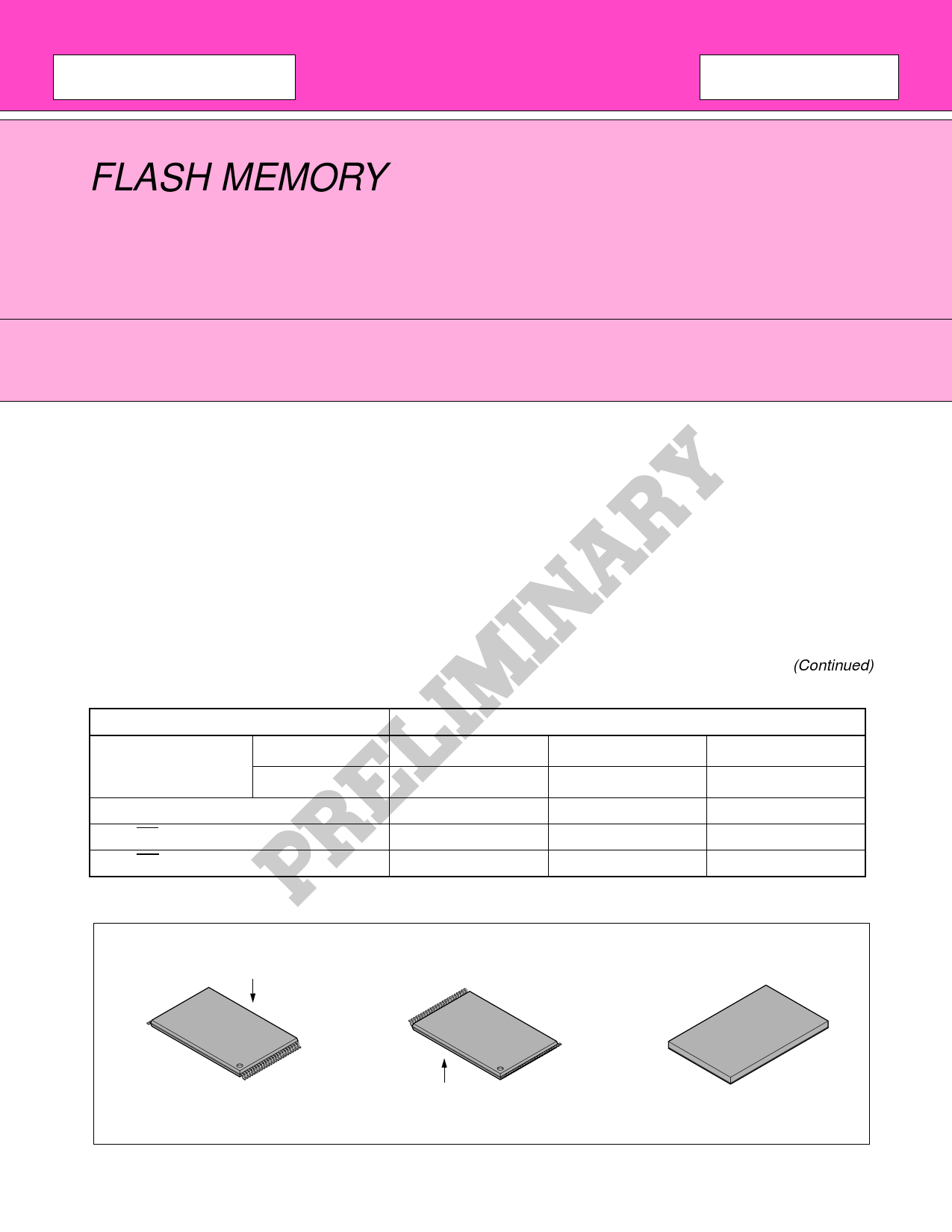
s PACKAGES
48-pin plastic TSOP (I)
Marking Side
48-pin plastic TSOP (I)
63-ball plastic FBGA
(FPT-48P-M19)
Marking Side
(FPT-48P-M20)
(BGA-63P-M01)
Share Link: 