MB88151A Просмотр технического описания (PDF) - Fujitsu
Номер в каталоге
Компоненты Описание
Список матч
MB88151A Datasheet PDF : 22 Pages
| |||
MB88151A
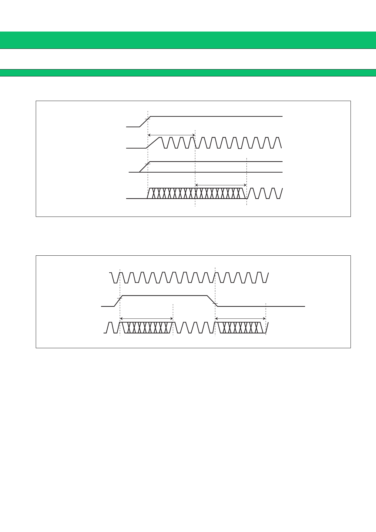
■ LOCK-UP TIME
3.0 V
VDD
Internal clock
stabilization wait time
XIN
Setting pin
VIH
SEL0,
SEL1,
ENS
CKOUT
tLK
(lock-up time )
If the setting pin is fixed at the “H” or “L” level, the maximum time after the power is turned on until the set clock
signal is output from CKOUT pin is (the stabilization wait time of input clock to XIN pin) + (the lock-up time “tLK”).
For the input clock stabilization time, check the characteristics of the resonator or oscillator used.
XIN
VIH
ENS
CKOUT
tLK
(lock-up time )
VIL
tLK
(lock-up time )
For modulation enable control using the ENS pin during normal operation, the set clock signal is output from
CKOUT pin at most the lock-up time (tLK) after the level at the ENS pin is determined.
Note : When the pin setting is changed, the CKOUT pin output clock stabilization time is required. Until the output
clock signal becomes stable, the output frequency, output clock duty cycle, modulation period, and cycle-
cycle jitter cannot be guaranteed. It is therefore advisable to perform processing such as cancelling a reset
of the device at the succeeding stage after the lock-up time.
15
Share Link: 