MAX8873 Просмотр технического описания (PDF) - Maxim Integrated
Номер в каталоге
Компоненты Описание
Список матч
MAX8873 Datasheet PDF : 8 Pages
| |||
Low-Dropout, 120mA Linear Regulators
______________________________________________________________Pin Description
PIN NAME
FUNCTION
1
IN
Regulator Input. Supply voltage can range from 2.5V to 6.5V. Bypass with 1µF to GND (see Capacitor
Selection and Regulator Stability).
2
GND
Ground. This pin also functions as a heatsink. Solder to large pads or the circuit board ground plane to max-
imize thermal dissipation.
3
SHDN
Active-Low Shutdown Input. A logic low reduces the supply current to 0.1nA. On the MAX8874, a logic low
also causes the output voltage to discharge to GND. Connect to IN for normal operation.
Feedback Input for Setting the Output Voltage. Connect to GND to set the output voltage to the preset 2.80V
4
SET
(MAX887_R), 2.84V (MAX887_S), or 3.15V (MAX887_T). Connect to an external resistor divider for
adjustable-output operation. DO NOT LEAVE THIS PIN UNCONNECTED.
5
OUT
Regulator Output. Fixed or adjustable from 1.25V to 6.5V. Sources up to 120mA. Bypass with a 1µF, <0.2Ω
typical ESR capacitor to GND.
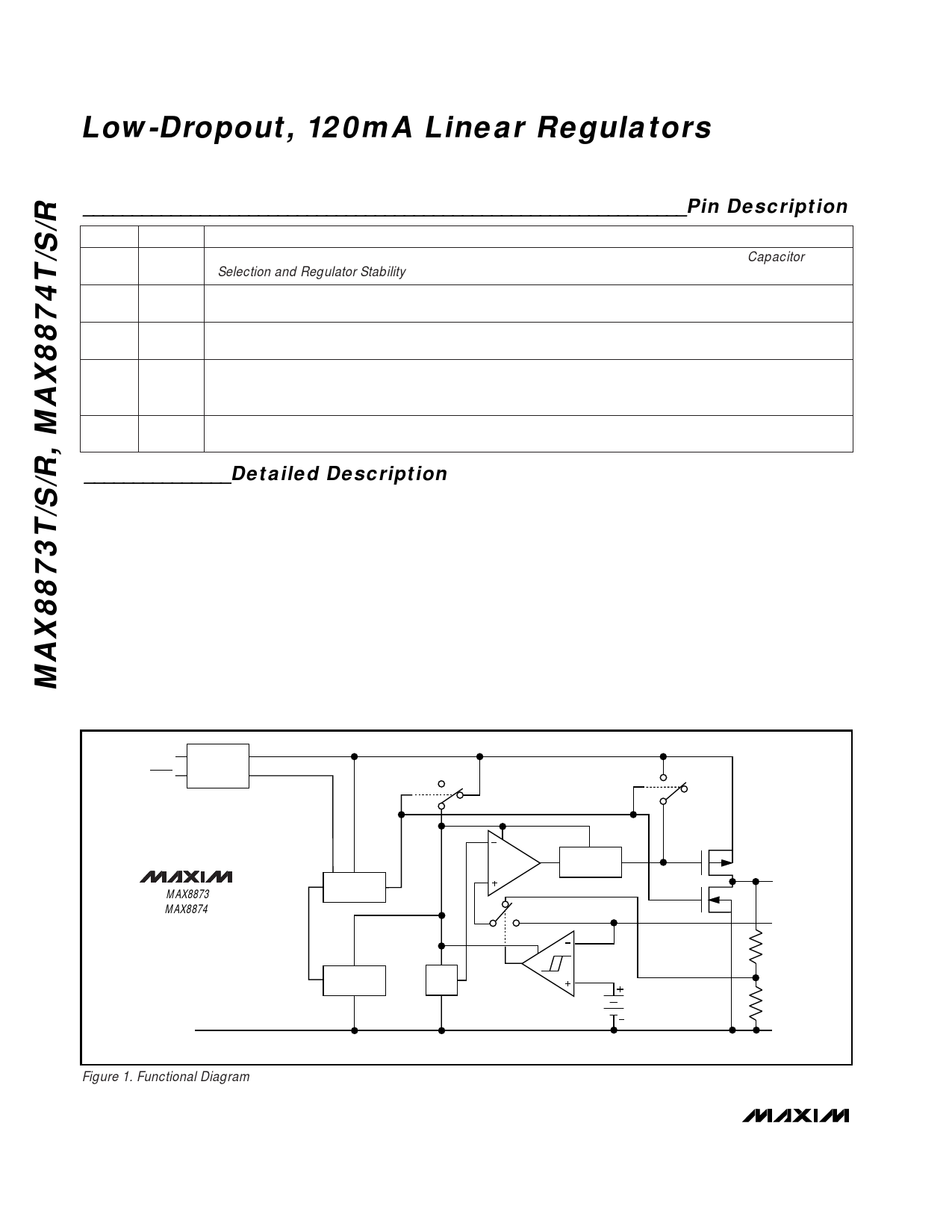
_______________Detailed Description
The MAX8873/MAX8874 are low-dropout, low-quiescent-
current linear regulators designed primarily for battery-
powered applications. They supply an adjustable 1.25V to
6.5V output or a preselected 2.80V (MAX887_R), 2.84V
(MAX887_S), or 3.15V (MAX887_T) output for load currents
up to 120mA. These devices consist of a 1.25V reference,
error amplifier, MOSFET driver, P-channel pass transistor,
dual-mode comparator, and internal feedback voltage
divider (Figure 1).
The 1.25V bandgap reference is connected to the error
amplifier’s inverting input. The error amplifier compares this
reference with the selected feedback voltage and amplifies
the difference. The MOSFET driver reads the error signal
and applies the appropriate drive to the P-channel pass
transistor. If the feedback voltage is lower than the refer-
ence, the pass-transistor gate is pulled lower, allowing more
current to pass and increasing the output voltage. If the
feedback voltage is too high, the pass-transistor gate is
pulled up, allowing less current to pass to the output.
The output voltage is fed back through either an internal
resistor voltage divider connected to the OUT pin, or an
external resistor network connected to the SET pin. The
dual-mode comparator examines the SET voltage and
selects the feedback path. If SET is below 60mV, internal
feedback is used and the output voltage is regulated to the
preset output voltage. Additional blocks include a current
limiter, reverse battery protection, thermal sensor, and shut-
down logic.
IN
SHDN
REVERSE
BATTERY
PROTECTION
MAX8873
MAX8874
SHUTDOWN
LOGIC
ERROR
AMP
MOS DRIVER
WITH ILIMIT
P
OUT
N
*
SET
THERMAL
SENSOR
1.25V
REF
GND
* AUTO-DISCHARGE, MAX8874 ONLY
Figure 1. Functional Diagram
DUAL-MODE
COMPARATOR
60mV
6 _______________________________________________________________________________________
Share Link: 