MAX8863(1998) Просмотр технического описания (PDF) - Maxim Integrated
Номер в каталоге
Компоненты Описание
Список матч
MAX8863 Datasheet PDF : 8 Pages
| |||
Low-Dropout, 120mA Linear Regulators
ABSOLUTE MAXIMUM RATINGS
VIN to GND ..................................................................-7V to +7V
Output Short-Circuit Duration ............................................Infinite
SET to GND ..............................................................-0.3V to +7V
SHDN to GND..............................................................-7V to +7V
SHDN to IN ...............................................................-7V to +0.3V
OUT to GND ................................................-0.3V to (VIN + 0.3V)
Continuous Power Dissipation (TA = +70°C)
SOT23-5 (derate 7.1mW/°C above +70°C) .................571mW
Operating Temperature Range ...........................-40°C to +85°C
Junction Temperature ......................................................+150°C
θJA ..............................................................................140°C/Watt
Storage Temperature Range .............................-65°C to +160°C
Lead Temperature (soldering, 10sec) .............................+300°C
Stresses beyond those listed under “Absolute Maximum Ratings” may cause permanent damage to the device. These are stress ratings only, and functional
operation of the device at these or any other conditions beyond those indicated in the operational sections of the specifications is not implied. Exposure to
absolute maximum rating conditions for extended periods may affect device reliability.
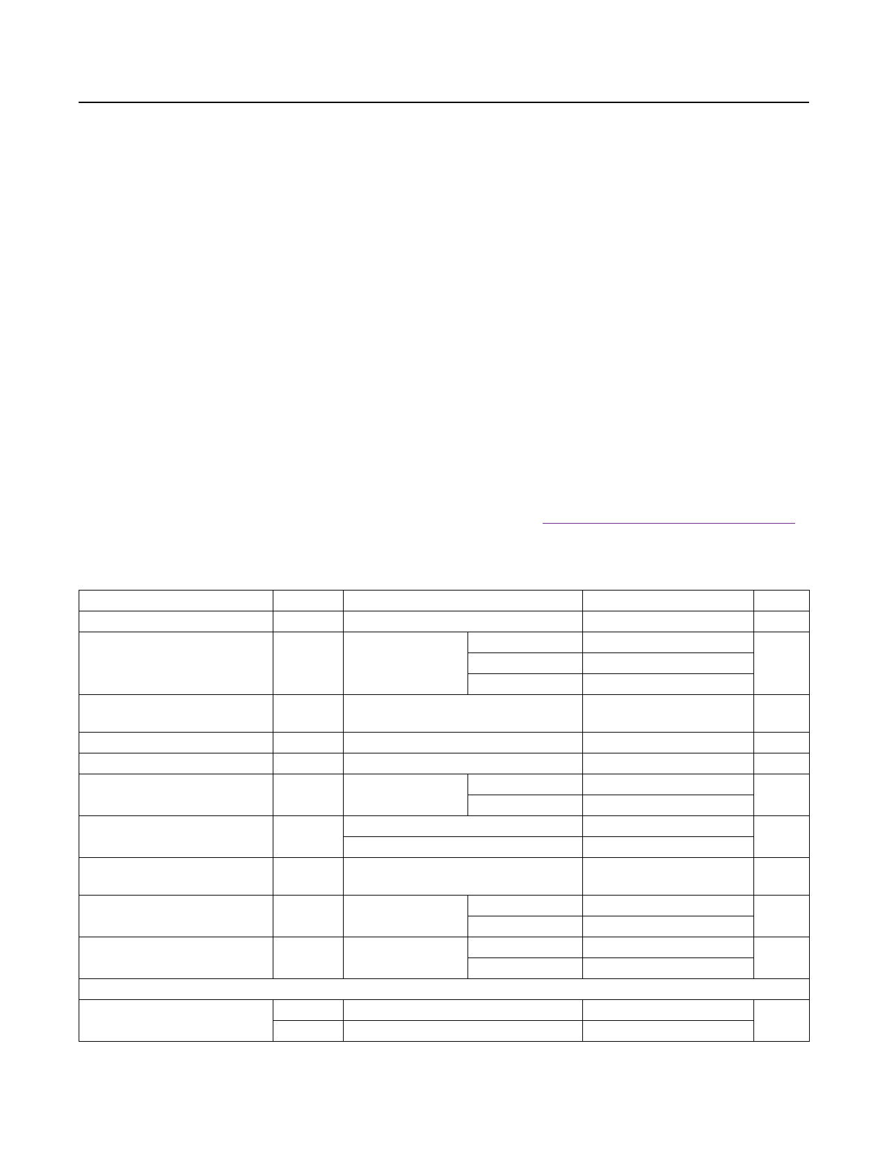
ELECTRICAL CHARACTERISTICS
(VIN = +3.6V, GND = 0V, TA = TMIN to TMAX, unless otherwise noted. Typical values are at TA = +25°C.) (Note 1)
PARAMETER
Input Voltage (Note 2)
Output Voltage
Adjustable Output Voltage
Range (Note 3)
Maximum Output Current
Current Limit (Note 4)
Ground Pin Current
Dropout Voltage (Note 5)
Line Regulation
Load Regulation
Output Voltage Noise
SHUTDOWN
SHDN Input Threshold
SHDN Input Bias Current
Shutdown Supply Current
Shutdown Discharge
Resistance (MAX8864)
SYMBOL
CONDITIONS
MIN
VIN
2.5
VOUT
0mA ≤ IOUT ≤ 50mA,
SET = GND
MAX886_T
3.05
MAX886_S
2.75
MAX886_R
2.70
VOUT
VSET
ILIM
IQ
∆VLNR
∆VLDR
120
SET = GND
IOUT = 1mA
IOUT = 50mA
ILOAD = 0mA
ILOAD = 50mA
VIN = 2.5V to 6.5V, SET tied to OUT,
IOUT = 1mA
IOUT = 0mA to 50mA
SET = GND
SET tied to OUT
10Hz to 1MHz
COUT = 1µF
COUT = 100µF
-0.15
TYP
3.15
2.84
2.80
280
68
80
1.1
55
0
0.011
0.006
350
220
MAX
6.5
3.25
2.93
2.88
UNITS
V
V
6.5
V
mA
mA
150
µA
mV
120
0.15 %/V
0.040
%/mA
µVRMS
VIH
VIL
ISHDN
VSHDN = VIN
IQSHDN VOUT = 0V
TA = +25°C
TA = TMAX
TA = +25°C
TA = TMAX
2.0
V
0.4
0
100
nA
0.05
0.0001 1
µA
0.02
300
Ω
2 _______________________________________________________________________________________
Share Link: 