MAX604 Просмотр технического описания (PDF) - Maxim Integrated
Номер в каталоге
Компоненты Описание
Список матч
MAX604 Datasheet PDF : 12 Pages
| |||
5V/3.3V or Adjustable, Low-Dropout,
Low IQ, 500mA Linear Regulators
Output Voltage Selection
The MAX603/MAX604 feature dual-mode operation. In
preset voltage mode, the output of the MAX603 is set to
5V and the output of the MAX604 is set to 3.3V using
internal, trimmed feedback resistors. Select this mode
by connecting SET to ground.
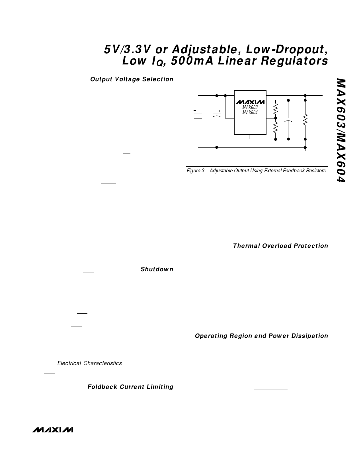
In adjustable mode, an output between 1.25V and 11V
is selected using two external resistors connected as a
voltage divider to SET (Figure 3). The output voltage is
set by the following equation:
VOUT = VSET 1 + RR21
where VSET = 1.20V. To simplify resistor selection:
R1
=
R2
VOUT
VSET
- 1
Since the input bias current at SET is nominally zero,
large resistance values can be used for R1 and R2 to
minimize power consumption without losing accuracy. Up
to 1.5MΩ is acceptable for R2. Since the VSET tolerance
is less than ±40mV, the output can be set using fixed
resistors instead of trim pots.
In preset voltage mode, impedances between SET and
ground should be less than 10kΩ. Otherwise, spurious
conditions could cause the voltage at SET to exceed
the 80mV dual-mode threshold.
Shutdown
A low input on the OFF pin shuts down the MAX603/
MAX604. In the off mode, the pass transistor, control
circuit, reference, and all biases are turned off, reduc-
ing the supply current below 2µA. OFF should be con-
nected to IN for normal operation.
Use a fast comparator, Schmitt trigger, or CMOS or TTL
logic to drive the OFF pin in and out of shutdown. Rise
times should be shorter than 1µs. Do not use slow RC
circuits, leave OFF open, or allow the input to linger
between thresholds; these measures will prevent the
output from jumping to the positive supply rail in
response to an indeterminate input state.
Since the OFF threshold varies with input supply volt-
age (see Electrical Characteristics), do not derive the
drive voltage from 3.3V logic. With VIN at 11.5V, the
high OFF logic level needs to be above 4V.
Foldback Current Limiting
The MAX603/MAX604 also include a foldback current
limiter. It monitors and controls the pass transistor’s
gate voltage, estimating the output current and limiting
it to 1.2A for output voltages above 0.8V and VIN - VOUT
IN
OUT
CIN
BATTERY 0.1µF to
10µF
MAX603
MAX604
OFF
SET
GND
OUTPUT
VOLTAGE
R1
COUT RL
10µF
R2
Figure 3. Adjustable Output Using External Feedback Resistors
> 0.7V. For VIN - VOUT < 0.7V (dropout operation), there
is no current limit. If the output voltage drops below
0.8V, implying a short-circuit condition, the output cur-
rent is limited to 350mA. The output can be shorted to
ground for one minute without damaging the device if
the package can dissipate VIN x 350mA without
exceeding TJ = +150°C.
Thermal Overload Protection
Thermal overload protection limits total power dissipa-
tion in the MAX603/MAX604. When the junction temper-
ature exceeds TJ = +160°C, the thermal sensor sends a
signal to the shutdown logic, turning off the pass tran-
sistor and allowing the IC to cool. The thermal sensor
will turn the pass transistor on again after the IC’s junc-
tion temperature cools by 10°C, resulting in a pulsed
output during thermal overload conditions.
Thermal overload protection is designed to protect the
MAX603/MAX604 in the event of fault conditions. For
continual operation, the absolute maximum junction tem-
perature rating of TJ = +150°C should not be exceeded.
Operating Region and Power Dissipation
Maximum power dissipation of the MAX603/MAX604
depends on the thermal resistance of the case and cir-
cuit board, the temperature difference between the die
junction and ambient air, and the rate of air flow. The
power dissipation across the device is P = IOUT (VIN -
VOUT). The resulting maximum power dissipation is:
( ( ) ) P MAX
=
TJ - TA
θJB + θBA
where (TJ - TA) is the temperature difference between
the MAX603/MAX604 die junction and the surrounding
_______________________________________________________________________________________ 7
Share Link: 