CS8129 Просмотр технического описания (PDF) - Cherry semiconductor
Номер в каталоге
Компоненты Описание
Список матч
CS8129 Datasheet PDF : 8 Pages
| |||
Absolute Maximum Ratings
Input Operating Range..................................................................................................................................................-0.5 to 26V
Power Dissipation.............................................................................................................................................Internally Limited
Peak Transient Voltage (46V Load Dump @ 14V VIN) ...............................................................................................-50V, 60V
Output Current .................................................................................................................................................Internally Limited
ESD Susceptibility (Human Body Model)..............................................................................................................................4kV
Junction Temperature .............................................................................................................................................-55¡C to 150¡C
Storage Temperature...............................................................................................................................................-55¡C to 150¡C
Lead Temperature Soldering
Wave Solder (through hole styles only) .....................................................................................10 sec. max, 260¡C peak
Reflow (SMD styles only) ......................................................................................60 sec. max above 183¡C, 230¡C peak
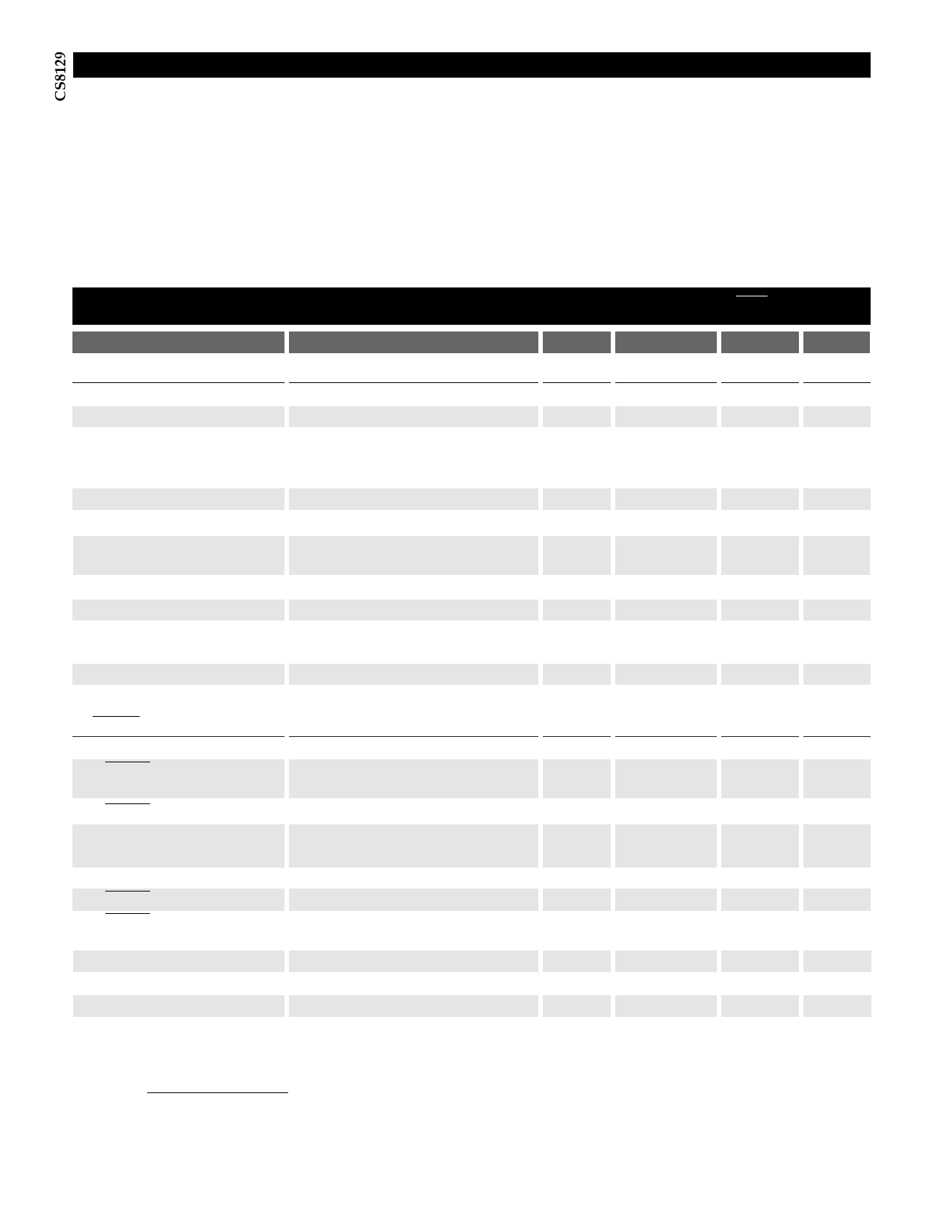
Electrical Characteristics: -40ûC ² TA ² + 125ûC, -40ûC ² TJ ² +150ûC, 6V ² VIN ² 26V, 5mA ² IOUT ² 500mA, R RESET = 4.7k½ to VOUT
unless otherwise noted*
PARAMETER
s Output Stage (VOUT)
Output Voltage
Dropout Voltage
Supply Current
Line Regulation
Load Regulation
Ripple Rejection
Current Limit
Overvoltage Shutdown
Reverse Polarity Input
Voltage DC
Thermal Shutdown
TEST CONDITIONS
IOUT = 500mA
IOUT ² 10mA
IOUT ² 100mA
IOUT ² 500mA
6V ² VIN ² 26V, IOUT = 50mA
50mA ² IOUT ² 500mA, VIN = 14V
f = 120Hz, VIN = 7 to 17V,
IOUT = 250mA
VOUT ³ -0.6V, 10½ Load
Guaranteed by Design
MIN
4.85
54
0.75
32
-15
150
TYP
5.00
0.35
2
6
55
5
10
75
1.20
-30
180
MAX
UNIT
5.15
V
0.60
V
7
mA
12
100
50
mV
50
mV
dB
A
40
V
V
210
¡C
s RESET and Delay Functions
Delay Charge Current
RESET Threshold
RESET Hysteresis
Delay Threshold
Delay Hysteresis
VDELAY = 2V
VOUT Increasing, VRT(ON)
VOUT Decreasing, VRT(OFF)
VRH=VRT(ON) - VRT(OFF)
Charge, VDC(HI)
Discharge, VDC(LO)
5
10
4.05
4.35
4.00
4.20
50
150
3.25
3.50
2.85
3.10
200
400
RESET Output Voltage Low1V < VOUT < VRT(L) , 3k½ to VOUT
0.1
RESET Output Leakage
VOUT > VRT(H)
0
Current
Delay Capacitor
Discharge Voltage
Delay Time
Discharge Latched ÒONÓ,
VOUT > VRT
CDELAY = 0.1µF (Note 1)
0.2
16
32
15
µA
4.50
V
4.45
V
250
mV
3.75
V
3.35
V
800
mV
0.4
V
10
µA
0.5
V
48
ms
* To observe safe operating junction temperatures, low duty cycle pulse testing is used in tests where applicable.
CDelay x VDelay Threshold Charge
Delay Time =
I Charge
= CDelay x 3.5 x 10⁵ (typ)
Note 1: assuming ideal capacitor
2
Share Link: 