MAS9271 Просмотр технического описания (PDF) - Micro Analog systems
Номер в каталоге
Компоненты Описание
Список матч
MAS9271 Datasheet PDF : 5 Pages
| |||
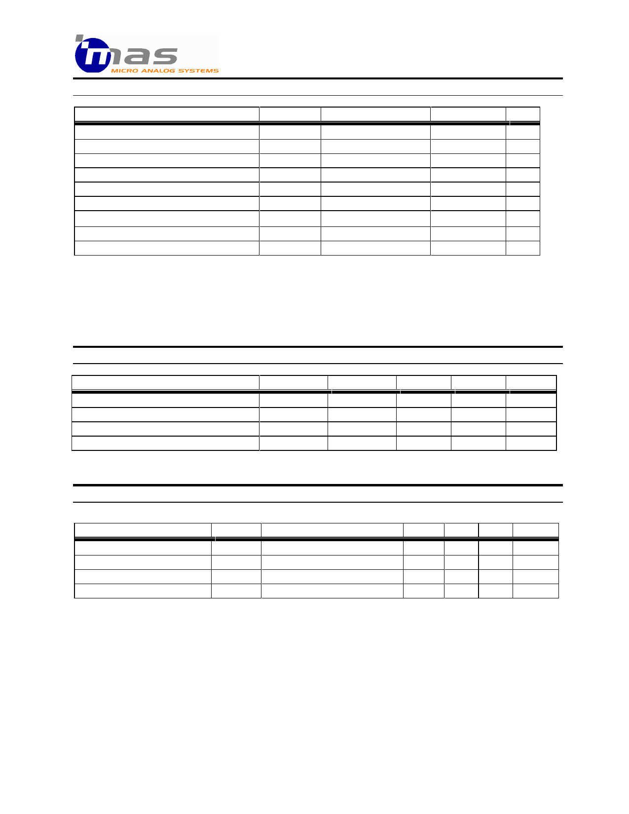
PIN DESCRIPTION
DA9271.005
13 July 2006
Pin Description
Power Supply Voltage
Crystal Oscillator Output
Crystal/Varactor Oscillator Input
Tri State
Serial Bus Clock Input
Serial Bus Data Input
Buffer Output
Power Supply Ground
Programming Input
Symbol
VDD
X1
X2
PD
CLK
DA
OUT
VSS
PV
x-coordinate
177
374
817
1012
201
435
665
830
1042
y-coordinate
172
158
158
158
1015
1015
1015
1008
1015
Note
Note: Also available in AK2140 pin order.
Note: Because the substrate of the die is internally connected to VDD, the die has to be connected to VDD or
left floating. Please make sure that VDD is the first pad to be bonded. Pick-and-place and all component
assembly are recommended to be performed in ESD protected area.
Note: Pad coordinates measured from the left bottom corner of the chip to the center of the pads. The
coordinates may vary depending on sawing width and location, however, distances between pads are accurate.
ABSOLUTE MAXIMUM RATINGS
Parameter
Supply Voltage
Input Voltage
Power Dissipation
Storage Temperature
Note: Not valid for programming pin PV
Symbol
VDD - VSS
VIN
PMAX
TST
Min
-0.3
VSS -0.3
-55
Max
6.0
VDD + 0.3
100
150
Unit
V
V
mW
oC
Note
1)
RECOMMENDED OPERATION CONDITIONS
Parameter
Supply Voltage
Supply Current
Operating Temperature
Crystal Load Capacitance
Symbol
VDD
ICC
TC
CL
Conditions
Vdd = 2.8 Volt
Min Typ Max Unit
2.5 2.8 5.5
V
2.3
mA
-40
+85
oC
8.0
pF
2 (5)
Share Link: 