SC16312 Просмотр технического описания (PDF) - Silan Microelectronics
Номер в каталоге
Компоненты Описание
Список матч
SC16312 Datasheet PDF : 12 Pages
| |||
Silan
Semiconductors
SC16312
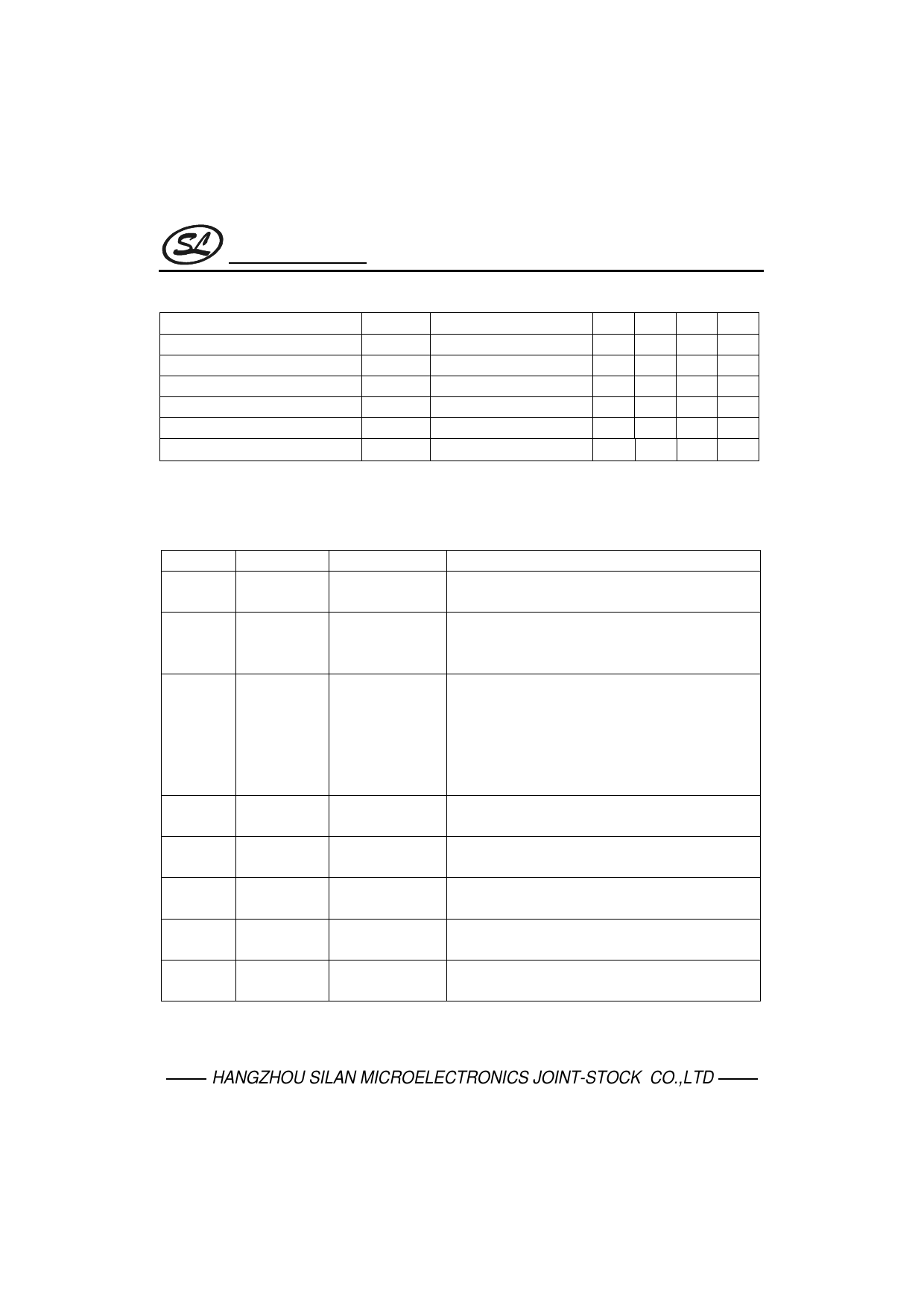
TIMING CONDITIONS(Ta=-20 ~ 70 °C, VDD =4.5 ~ 5.5V)
Parameter
Symbol
Test conditions
Min Typ Max Unit
Clock Pulse Width
PWCLK
--
400 --
--
ns
Strobe Pulse Width
PWSTB
--
1
--
--
µs
Data Setup Time
tSETUP
--
100 --
--
ns
Data Hold Time
tHOLD
--
100 --
--
ns
Clock-Strobe Time
Wait Time
tCLK-STB
tWAT
CLK ↑ → STB ↑
CLK ↑ → CLK ↓ Note
1
--
--
µs
1
--
--
µs
Note: When data is read, a wait time tWAIT of 1 µs is necessary since the rising of the eighth clock that has set the
command, until the falling of the first clock that has read the data.
PAD DESCRIPTION
Pin No.
Symbol
6
DIN
5
DOUT
9
STB
8
CLK
44
15 ~ 20
21 ~ 25
OSC
Seg1/KS1
to Seg6/KS6
Seg7 to Seg11
37 ~ 32 Grid1 to Grid6
Pin Name
Data input
Data output
Strobe
Clock input
Oscillator pin
Description
Input serial data at rising edge of shift clock, starting from
the low order bit.
Output serial data at the falling edge of the shift clock,
starting from low order bit. This is N-ch open-drain output
pin.
Initializes serial interface at the rising or falling edge of
the SC16312. It then waits for reception of a command.
Data input after STB has fallen is processed as a
command. While command data is processed, current
processing is stopped, and the serial interface is
initialized. While STB is high, CLK is ignored.
Reads serial data at the rising edge, and outputs data at
the falling edge.
Connect resistor to this pin to determine the oscillation
frequency to this pin.
High-voltage output Segment output pins (Dual function as key source).
High-voltage output
(segment)
High-voltage output
(grid)
Segment output pins.
Grid output pins.
(to be continued)
HANGZHOU SILAN MICROELECTRONICS JOINT-STOCK CO.,LTD
Rev: 1.0 2000.12.31
5
Share Link: 