M38C88EA-XXXFP Просмотр технического описания (PDF) - MITSUBISHI ELECTRIC
Номер в каталоге
Компоненты Описание
Список матч
M38C88EA-XXXFP Datasheet PDF : 51 Pages
| |||
PRELIMINARY NSocothimcaene:gpTeah.riasmisetnrioct laimfiintsalasrepescuibfijceacttioton.
MITSUBISHI MICROCOMPUTERS
38C8 Group
SINGLE-CHIP 8-BIT CMOS MICROCOMPUTER
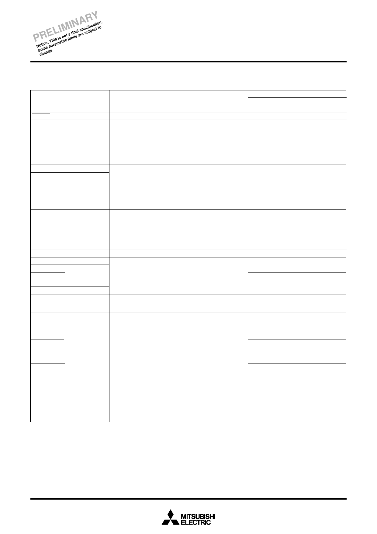
PIN DESCRIPTION
Table 1 Pin description
Pin
VCC, VSS
RESET
XIN
Name
Power source
Reset input
Clock input
XOUT
Clock output
OSCSEL
XCIN
XCOUT
RC oscillation
select
Sub-clock input
Sub-clock output
VLIN
Power source
input for LCD
VL1 – VL5
LCD power
source
COM0 –
COM32
Common output
SEG0/COM16– Segment output/
SEG7/COM23, Common output
SEG60COM31–
SEG67/COM24
SEG8–SEG59 Segment output
P00–P07
I/O port P0
P14–P17
I/O port P1
P10/AIN4–
P13/AIN7
P20–P27
I/O port P2
P30/AIN0 – I/O port P3
P33/AIN3
P40/INT0
Input port P4
P41/INT1/ADT I/O port P4
P42/CNTR0/
BEEP+,
P43/CNTR1/
BEEP-
P44/RxD,
P45/TxD,
P46/SCLK,
P47/SRDY
C1,
Voltage multiplier
C2,
C3
VSS (NC), NC
Function
Function except a port function
• Apply voltage of 4.0–5.5 V to VCC, and 0 V to VSS. (at high-speed mode)
• Reset input pin for active “L.”
• Input and output pins for the main clock generating circuit.
• Feedback resistor is built in between XIN pin and XOUT pin.
• Connect a ceramic resonator or a quartz-crystal oscillator between the XIN and XOUT pins to set the
oscillation frequency.
• If an external clock is used, connect the clock source to the XIN pin and leave the XOUT pin open.
• This pin determines the oscillation between XIN and XOUT. The oscillation method can be selected from
either by an oscillator or by a resistor.
• Input and output pins for sub-clock generating circuit. (Connect a quartz-crystal oscillator between the
XCIN and XCOUT pins to set the oscillation frequency. The clock generated the externals cannot be input
directly.)
• Reference voltage input pin for LCD.
• The input voltage to this pin is boosted threefold by voltage multiplier.
• LCD drive power source pins.
• LCD common output pins.
• LCD segment/common output pins.
• LCD segment output pins.
• 8-bit I/O port.
• CMOS compatible input level.
• CMOS 3-state output structure.
• 4-bit I/O port.
• CMOS compatible input level.
• CMOS 3-state output structure.
• 1-bit input port.
• CMOS compatible input level.
• 7-bit I/O port.
• CMOS compatible input level.
• CMOS 3-state output structure.
• I/O direction register allows each pin to be individually
programmed as either input or output.
• A-D converter analog input pin
• Key-on wake-up interrupt input pin
• A-D converter analog input pin
• External interrupt pin
• External interrupt pin
• A-D trigger input pin
•Timer function I/O pin
• Serial I/O I/O pin
• External capacitor connect pins for a voltage multiplier of LCD.
• Non-function pins.
• Leave the VSS (NC) pin open.
4
Share Link: 