M37640E8FP Просмотр технического описания (PDF) - Mitsumi
Номер в каталоге
Компоненты Описание
Список матч
M37640E8FP Datasheet PDF : 96 Pages
| |||
Ver 1.4
MITSUBISHI MICROCOMPUTERS
7640 Group
SINGLE-CHIP 8-BIT CMOS MICROCOMPUTER
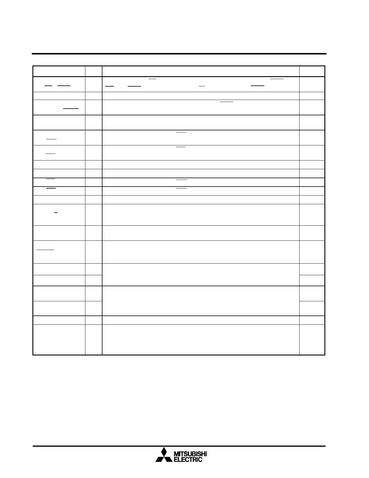
NAME
P73/IBF1/HLDA
P74/OBF1
P80/UTXD2/SRDY
P81/URXD2/SCLK
P82/CTS2/SRXD
P83/RTS2/STXD
P84/UTXD1
P85/URXD1
P86/CTS1
P87/RTS1
AVcc, AVss
CNVss/Vpp
Vcc,Vss
RESET
XCin
XCout
Xin
Xout
LPF
Ext. Cap
I/O
DESCRIPTION
CMOS I/O port or IBF1 output to master CPU for data bus buffer 1, or HLDA pin.
I/O IBF1 and HLDA are mutually exclusive. IBF 1 has priority over HLDA
I/O CMOS I/O port or OBF1 output to master CPU for data bus buffer 1.
CMOS I/O port or UART2 pin UTXD2 or SIO pin SRDY. UART2 and SIO are
I/O mutually exclusive, UART2 has priority over SIO.
CMOS I/O port or UART2 pin URXD2 or SIO pin SCLK. UART2 and SIO are
I/O mutually exclusive, UART2 has priority over SIO.
CMOS I/O port or UART2 pin CTS2 or SIO pin SRXD. UART2 and SIO are
I/O mutually exclusive, UART2 has priority over SIO.
CMOS I/O port or UART2 pin RTS2 or SIO pin STXD. UART2 and SIO are
I/O mutually exclusive, UART2 has priority over SIO.
I/O CMOS I/O port or UART1 pin UTXD1.
I/O CMOS I/O port or UART1 pin URXD1.
I/O CMOS I/O port or UART1 pin CTS1.
I/O CMOS I/O port or UART1 pin RTS1.
I Power supply inputs for analog circuitry AVcc = 4.15~ 5.25V, AVss = 0V
Controls the processor mode of the chip. Normally connected to Vss or Vcc.
I When the MCU is in EPROM program mode, this pin supplies the programming
voltage to the EPROM.
I Power supply inputs: Vcc = 4.15~ 5.25V, Vss = 0V
To enter the reset state, this pin must be kept 'L' for more that 2µs (20 Φ cycles
I under normal Vcc conditions). If the crystal or ceramic resonator requires more
time to stabilize, extend this 'L' level time appropriately.
I An external ceramic or quartz crystal oscillator can be connected between the
O
XCin and XCout pins. If an external clock source is used, connect the clock
source to the XCin pin and leave the XCout pin open.
Input and output signals to and from the internal clock generation circuit.
I Connect a ceramic resonator or quartz crystal between Xin and Xout pins to set
O the oscillation frequency. If an external clock is used, connect the clock source
to the Xin pin and leave the Xout pin open.
O Loop filter for the frequency synthesizer.
An external capacitor (Ext. Cap) pin. When the USB transceiver voltage
I converter is used, a 2µf or larger capacitor should connect between this pin and
Vss to ensure proper operation of the USB line driver. The voltage converter is
enabled by setting bit 4 of the USB control register (001316) to a “1”.
PIN #
66
65
32
31
30
29
28
27
26
25
17,19
9
16/74
13/73
10
12
11
14
15
18
72
4
Share Link: 