M37516M6-A05 Просмотр технического описания (PDF) - Mitsumi
Номер в каталоге
Компоненты Описание
Список матч
M37516M6-A05 Datasheet PDF : 54 Pages
| |||
FUNCTIONAL DESCRIPTION
CENTRAL PROCESSING UNIT (CPU)
The M37516M6-XXXHP uses the standard 740 Family instruction
set. Refer to the table of 740 Family addressing modes and ma-
chine instructions or the 740 Family Software Manual for details
on the instruction set.
Machine-resident 740 Family instructions are as follows:
The FST and SLW instructions cannot be used.
The STP, WIT, MUL, and DIV instructions can be used.
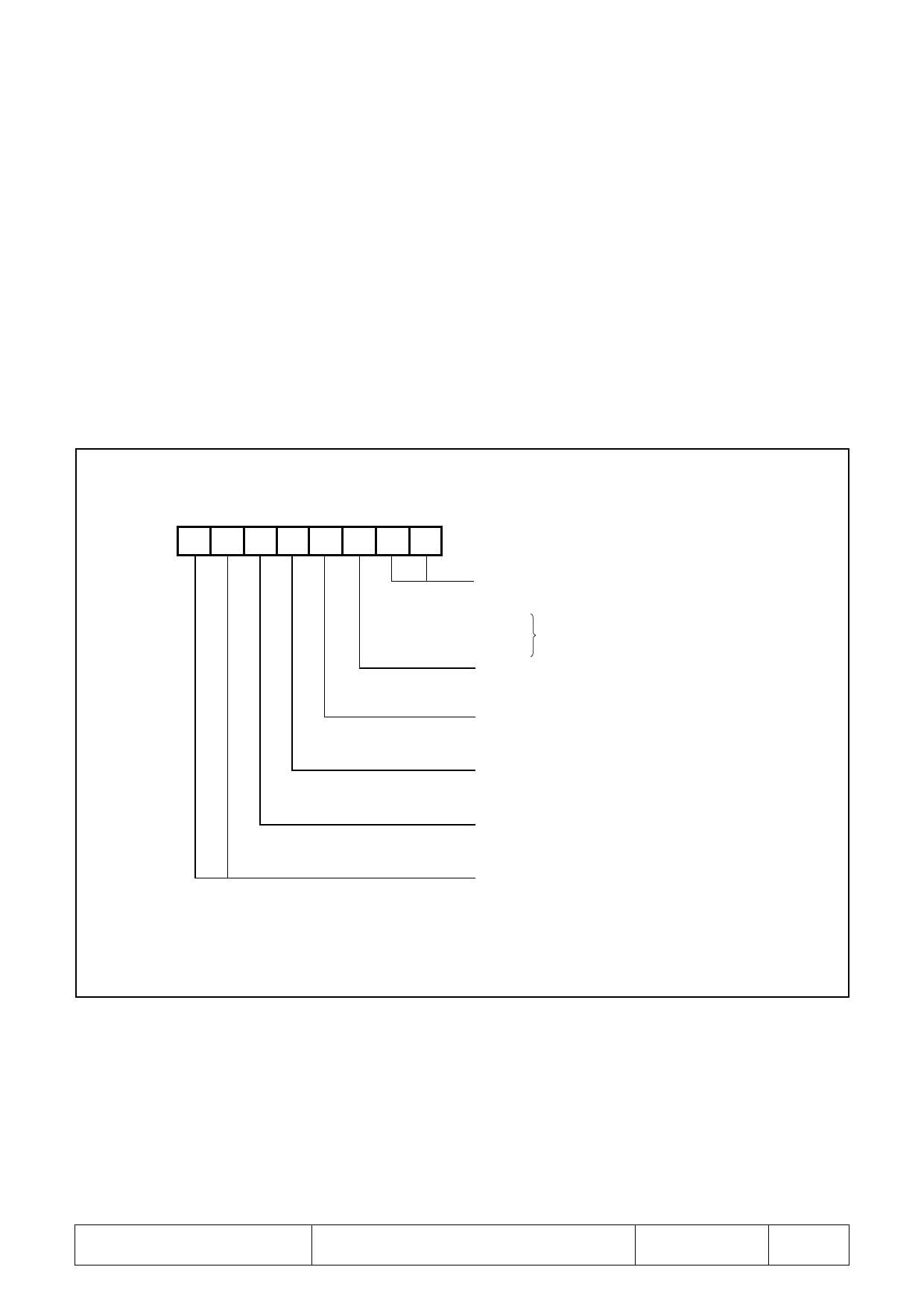
[CPU Mode Register (CPUM)] 003B16
The CPU mode register contains the stack page selection bit, etc.
The CPU mode register is allocated at address 003B16.
b7
Fig. 3 Structure of CPU mode register
b0
CPU mode register
(CPUM : address 003B16)
Processor mode bits
b1 b0
0 0 : Single-chip mode
0 1:
1 0 : Not available
1 1:
Stack page selection bit
0 : 0 page
1 : 1 page
Not used (return “1” when read)
(Do not write “0” to this bit.)
Port XC switch bit
0 : I/O port function (stop oscillating)
1 : XCIN–XCOUT oscillating function
Main clock (X IN–XOUT) stop bit
0 : Oscillating
1 : Stopped
Main clock division ratio selection bits
b7 b6
0 0 : φ = f(XIN)/2 (high-speed mode)
0 1 : φ = f(XIN)/8 (middle-speed mode)
1 0 : φ = f(XCIN)/2 (low-speed mode)
1 1 : Not available
M37516M6-XXXHP
GNOK-M37516M6-XXXHP-50
(MSETSU 2)
PA
GE
5/54
Share Link: 