M36W216TI85ZA1T Просмотр технического описания (PDF) - STMicroelectronics
Номер в каталоге
Компоненты Описание
Список матч
M36W216TI85ZA1T
STMicroelectronics

M36W216TI85ZA1T Datasheet PDF : 62 Pages
| |||
M36W216TI, M36W216BI
VSSF and VSSS Ground. VSSF and VSSS are the
ground reference for all voltage measurements in
the Flash and SRAM chips, respectively.
Note: Each device in a system should have VD-
DF, VDDQF and VPPF decoupled with a 0.1µF ca-
pacitor close to the pin. See Figure 9, AC
Measurement Load Circuit. The PCB trace
widths should be sufficient to carry the re-
quired VPPF program and erase currents.
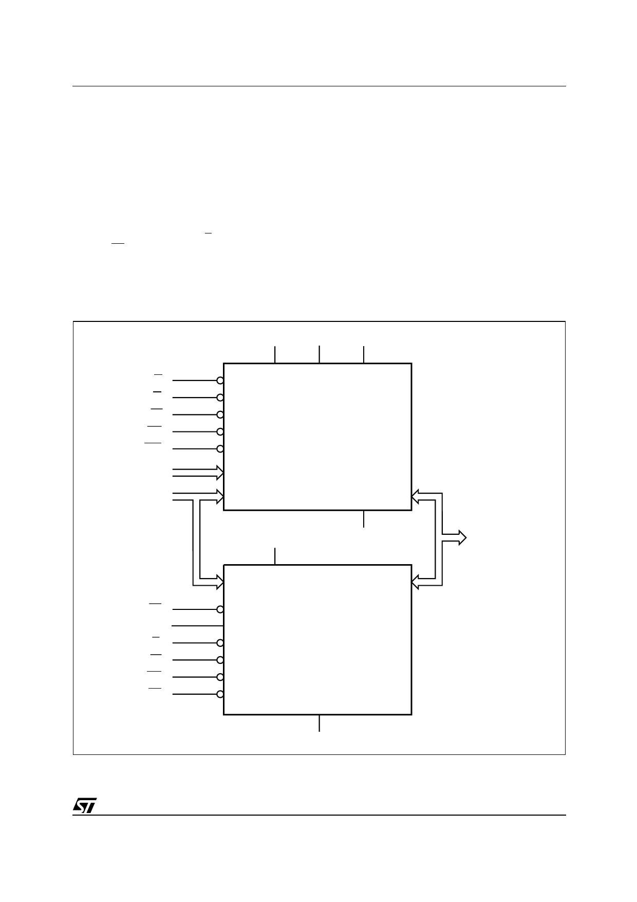
FUNCTIONAL DESCRIPTION
The Flash and SRAM components have separate
power supplies and grounds and are distinguished
by three chip enable inputs: EF for the Flash mem-
ory and E1S and E2S for the SRAM.
Recommended operating conditions do not allow
both the Flash and the SRAM to be in active mode
at the same time. The most common example is
simultaneous read operations on the Flash and
the SRAM which would result in a data bus con-
tention. Therefore it is recommended to put the
SRAM in the high impedance state when reading
the Flash and vice versa (see Table 2 Main Oper-
ation Modes for details).
Figure 4. Functional Block Diagram
VDDF
VDDQF
VPPF
EF
GF
WF
RPF
WPF
A17-A19
A0-A16
Flash Memory
16 Mbit (x16)
VDDS
VSSF
DQ0-DQ15
E1S
E2S
GS
WS
UBS
LBS
SRAM
2 Mbit (x16)
VSSS
AI07904
9/62
Share Link: