M30240F3 Просмотр технического описания (PDF) - Mitsumi
Номер в каталоге
Компоненты Описание
Список матч
M30240F3 Datasheet PDF : 142 Pages
| |||
Preliminary Specifications REV. E
Specifications in this manual are tentative and subject to change
Mitsubishi microcomputers
M30240 Group
Performance outline
SINGLE-CHIP 16-BIT CMOS MICROCOMPUTER
1.5 Performance outline
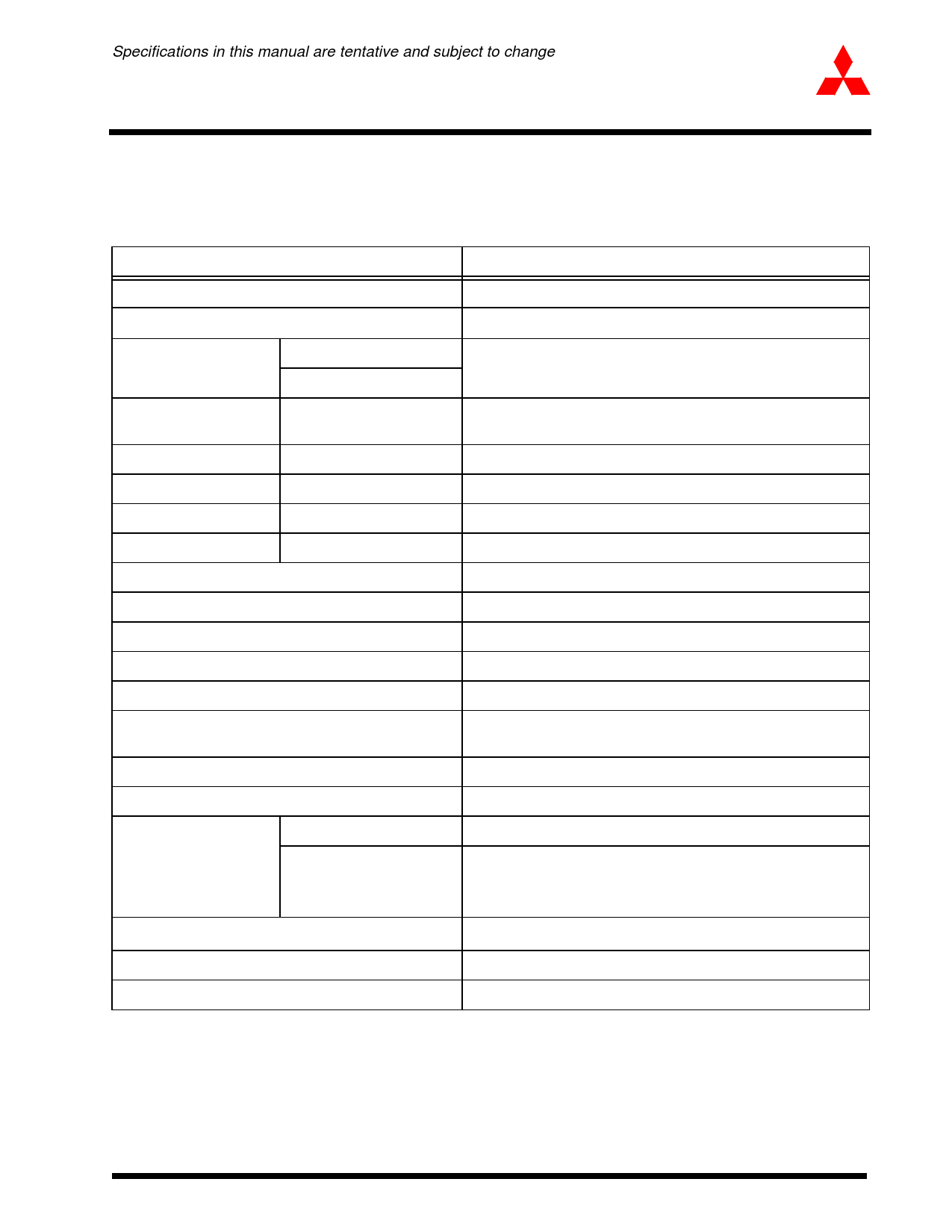
Table 1.1 is a performance outline of the M30240 group.
Table 1.1: Performance outline of M30240 group
Item
Number of basic instructions
91 instructions
Performance
Shortest instruction execution time
Memory capacity
ROM
RAM
I/O port
P0 to P3, P6,P7, P8
(except P85), P10
Input port
P85
Multifunction Timer
TA0, TA1, TA2, TA3, TA4
General purpose Timer TB0, TB1, TB2
Serial I/O
UART0, UART1, UART2
A-D converter
DMAC
CRC calculation circuit
Watchdog timer
Interrupt
Clock-generating circuit
Supply voltage (typical)
Power consumption (typical)
I/O withstand voltage
I/O characteristics
Average output current
Operating temperature
Device configuration
Package
83ns (f(XIN) =12MHz)
(See Figure 3: ROM capacity field)
8 bits x 7, 7 bits x 1
1 bit x 1
16 bits x 5
16 bits x 3
(UART or clock synchronous) x 3
10 bits x 8 channels
2 channels (trigger:18 sources)
CRC-CCITT
15 bits x 1 (with prescaler)
21 internal and 4 external sources, 4 software sources, 7 levels
Built-in clock generation circuit (built-in feedback resistor, and
external ceramic or quartz oscillator)
4.1 to 5.25V, (f(XIN)=12MHz, without software wait)
250 mwatt, Vcc=5.0V, 12MHz
5V
5 mA available on ports P0, P1, P3,P6, P71, P73, P75, P77,
P81~P84, P86, P87, P10
10 mA available on ports P2, P70, P72, P74, P76, P80
0 to 70oC
CMOS high performance silicon gate
80-pin plastic molded QFP
1-6
Share Link: 