LX8415-00 Просмотр технического описания (PDF) - Microsemi Corporation
Номер в каталоге
Компоненты Описание
Список матч
LX8415-00 Datasheet PDF : 7 Pages
| |||
LX8415-xx
PRODUCT DATABOOK 1996/1997
0.5A LOW DROPOUT POSITIVE REGULATORS
PR E L I M I N A RY D ATA S H E E T
A B S O L U T E M A X I M U M R AT I N G S (Note 1)
Power Dissipation .................................................................................. Internally Limited
Input Voltage
LX8415-00 (Adjustable) / 8415-33 (3.3V) .................................................................. 7V
Surge Voltage ................................................................................................................. 7V
Operating Junction Temperature
Plastic (ST, DD & DT Packages) .......................................................................... 150°C
Storage Temperature Range ...................................................................... -65°C to 150°C
Lead Temperature (Soldering, 10 seconds) ............................................................. 300°C
Short-Circuit Protection ....................................................................................... Indefinite
Note 1. Exceeding these ratings could cause damage to the device. All voltages are with
respect to Ground. Currents are positive into, negative out of the specified terminal.
T H E R MAL DATA
ST PACKAGE:
THERMAL RESISTANCE-JUNCTION TO TAB, θJT
THERMAL RESISTANCE-JUNCTION TO AMBIENT, θJA
15°C/W
*150°C/W
Junction Temperature Calculation: T = T + (P x θ ). The θ numbers are guidelines for the
J
A
D
JA
JA
thermal performance of the device/pc-board system. All of the above assume no ambient airflow.
* θJAcan be improved with package soldered to 0.5IN2 copper area over backside ground
plane or internal power plane. θJAcan vary from 20ºC/W to > 40ºC/W depending on
mounting technique. (See Application Notes Section: Thermal Considerations)
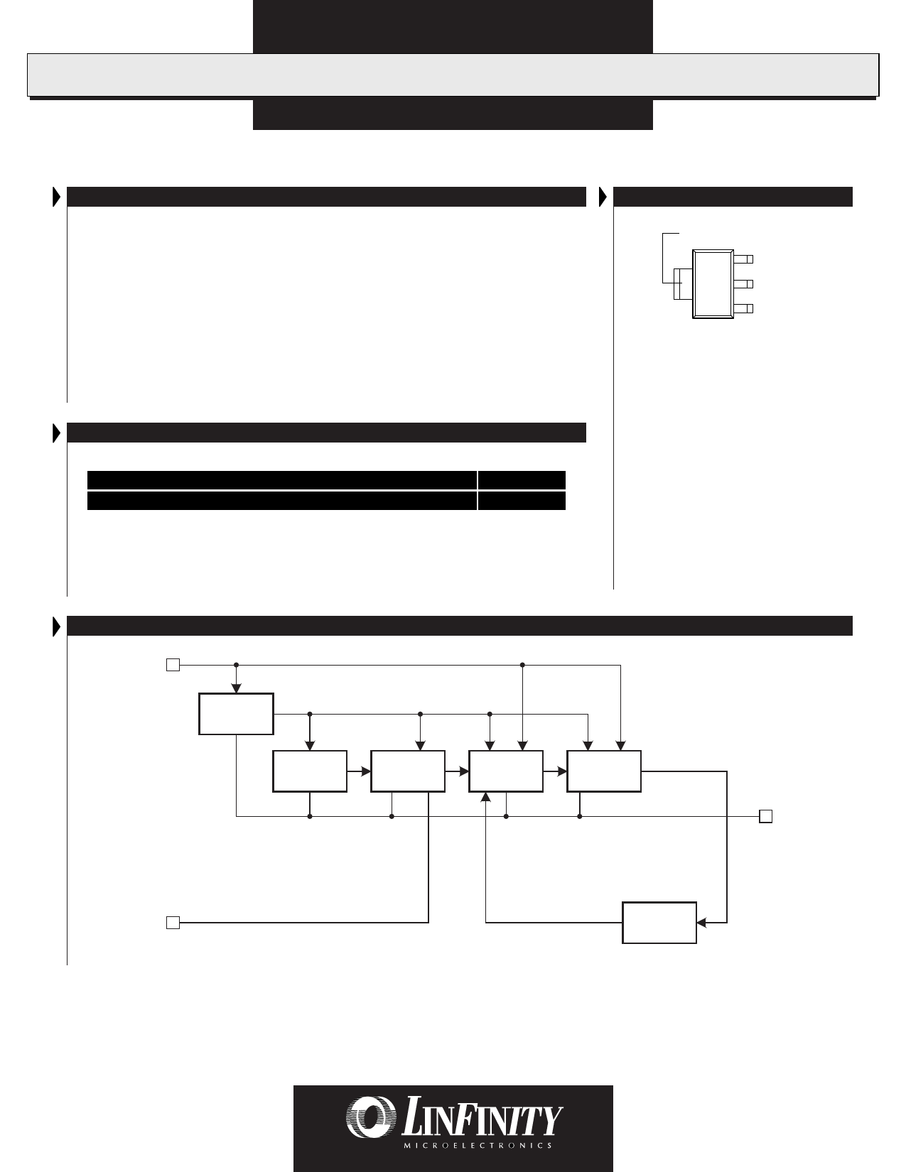
BLOCK DIAGRAM
VIN
Bias
Circuit
Thermal
Limit Circuit
Bandgap
Circuit
Control
Circuit
Output
Circuit
PACKAGE PIN OUTS
TAB IS VOUT
3. IN
2. OUT
1. ADJ / GND
ST PACKAGE
(Top View)
VOUT
ADJ
Current
Limit Circuit
2
Copyright © 1999
Rev. 0.4 1/99
Share Link: 