LX8384B-00CPT Просмотр технического описания (PDF) - Microsemi Corporation
Номер в каталоге
Компоненты Описание
Список матч
LX8384B-00CPT Datasheet PDF : 11 Pages
| |||
LX8384x-xx
TM
®
5A Low Dropout Positive Regulators
PRODUCTION DATA SHEET
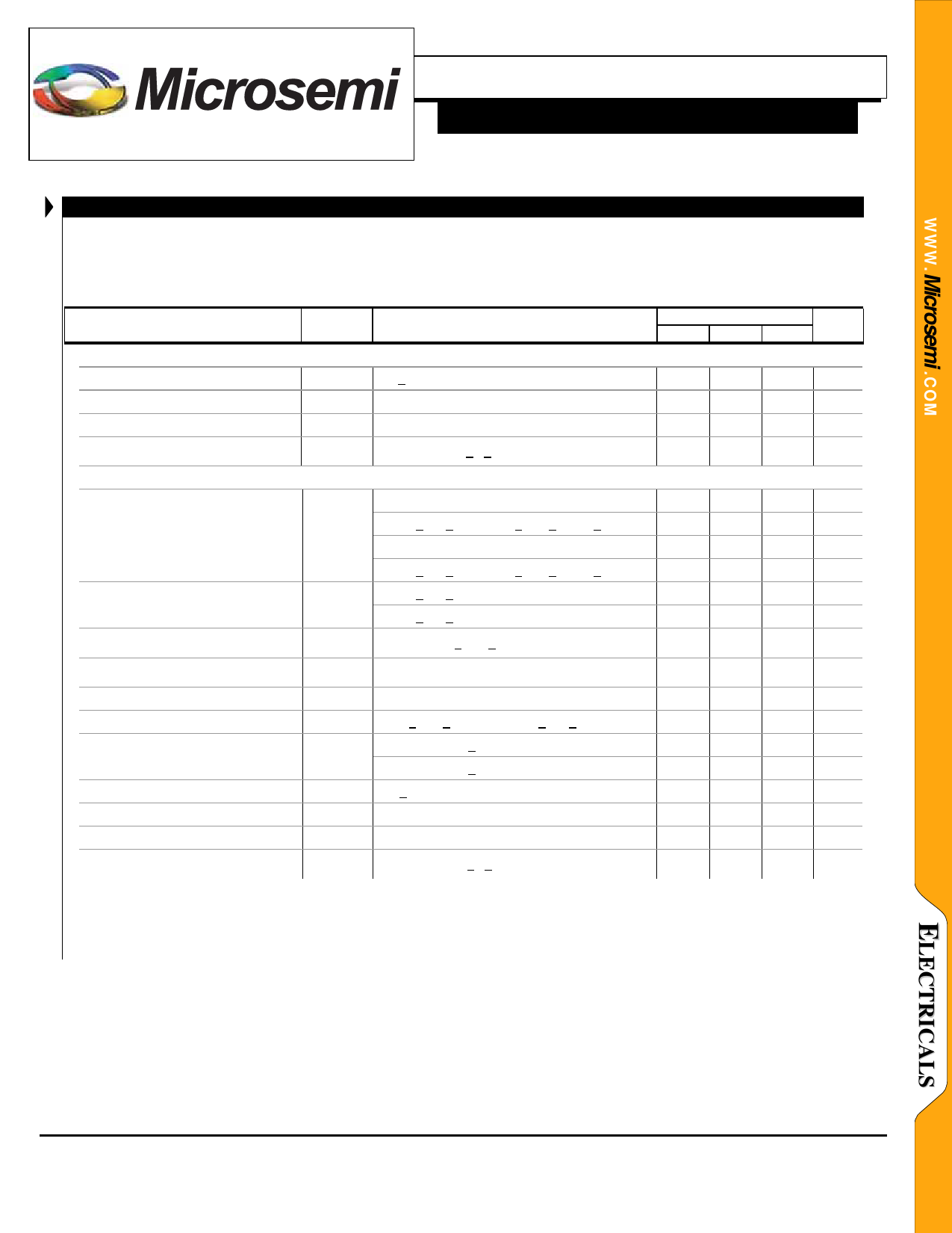
ELECTRICAL CHARACTERISTICS (CONTINUED)
Unless otherwise specified, the following specifications apply over the operating ambient temperature for the LX8384x-xxC with
0°C ≤ TA ≤ 125°C and the LX8384-xxI with -25°C ≤ TA ≤ 125°C except where otherwise noted. Test conditions: VIN -VOUT = 3V;
IOUT = 5A. Low duty cycle pulse testing techniques are used which maintains junction and case temperatures equal to the ambient
temperature.
Parameter
Symbol
Test Conditions
` LX8384-15 / 8384A-15 / 8384B-15 (1.5V FIXED)(CONTINUED)
Maximum Output Current
IOUT(MAX) VIN < 7V
Temperature Stability (Note 3)
ΔVOUT(T)
Long Term Stability (Note 3)
ΔVOUT (t) TA=125°C, 1000 hours
RMS Output Noise (% of VOUT)
(Note 3)
VOUT (RMS) TA=25°C, 10Hz < f < 10kHz
` LX8384-33 / 8384A-33 / 8384B-33 (3.3V FIXED)
Output Voltage
(Note 4)
LX8384/84A-33
LX8384B-33
VOUT
VIN=5V, IOUT=0mA, TA=25°C
4.75V < VIN < 10V, 0mA < IOUT < 5A, P < PMAX
VIN=5V, IOUT=0mA, TA=25°C
4.75V < VIN < 10V, 0mA < IOUT < 5A, P < PMAX
Line Regulation (Note 2)
Load Regulation (Note 2)
Thermal Regulation
Ripple Rejection (Note 3)
4.75V < VIN < 7V
ΔVOUT(VIN)
4.75V < VIN < 10V
ΔVOUT
(IOUT)
ΔVOUT
(Pwr)
VIN=5V, 0mA < IOUT < IOUT(MAX)
TA=25°C, 20ms pulse
COUT=100µF (Tantalum), IOUT=5A
Quiescent Current
IQ
0mA < IOUT < IOUT(MAX), 4.75V < VIN < 10V
Dropout Voltage LX8384-33
ΔVOUT=1%, IOUT < IOUT(MAX)
ΔV
LX8384A/84B-33
ΔVOUT=1%, IOUT < IOUT(MAX)
Maximum Output Current
IOUT(MAX) VIN < 7V
Temperature Stability (Note 3)
ΔVOUT (T)
Long Term Stability (Note 3)
RMS Output Noise (% of VOUT)
(Note 3)
ΔVOUT (t) TA=125°C, 1000 hours
VOUT (RMS) TA=25°C, 10Hz < f < 10kHz
LX8384x-xx
Units
Min Typ Max
5
6
A
0.25
%
0.3
1
%
0.003
%
3.267 3.30 3.333 V
3.235 3.30 3.365 V
3.274 3.30 3.326 V
3.267 3.30 3.333 V
1
6
mV
2
10
mV
5
15
mV
0.01 0.02 % / W
60
83
dB
4
10
mA
1.2
1.5
V
1
1.3
V
5
6
A
0.25
%
0.3
1
%
0.003
%
Note 2
Note 3
Note 4
Regulation is measured at constant junction temperature, using pulse testing with a low duty cycle. Changes in output
voltage due to heating effects are covered under the specification for thermal regulation.
These parameters, although guaranteed are not tested in production.
See Maximum Output Current Section
Copyright © 2000
Rev. 2.1f, 2006-01-20
Microsemi Inc.
Integrated Products Division
11861 Western Avenue, Garden Grove, CA. 92841, 714-898-8121, Fax: 714-893-2570
Page 4
Share Link: 