LT3798IMSE-PBF Просмотр технического описания (PDF) - Linear Technology
Номер в каталоге
Компоненты Описание
Список матч
LT3798IMSE-PBF Datasheet PDF : 20 Pages
| |||
LT3798
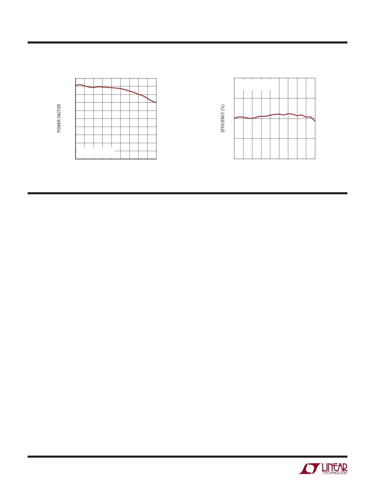
TYPICAL PERFORMANCE CHARACTERISTICS TA = 25°C, unless otherwise noted.
Power Factor vs Input Voltage
1.00
0.99
0.98
0.97
0.96
0.95
0.94
0.93
0.92
0.91 PAGE 17 SCHEMATIC:
UNIVERSAL
0.90
90 110 130 150 170 190 210 230 250 270
VIN (VAC)
3798 G15
Efficiency vs Input Voltage
100
PAGE 17 SCHEMATIC:
UNIVERSAL
90
80
70
60
90 110 130 150 170 190 210 230 250 270
VIN (VAC)
3798 G16
PIN FUNCTIONS
CTRL1, CTRL2, CTRL3 (Pin 1, Pin 2, Pin 3): Current
Output Adjustment Pins. These pins control the output
current. The lowest value out of the three CTRL inputs is
compared to negative input of the operational amplifier.
VREF (Pin 4): Voltage Reference Output Pin. Typically 2V.
This pin drives a resistor divider for the CTRL pin, either
for analog dimming or for temperature limit/compensation
of output load. Can supply up to 200µA.
OVP (Pin 5): Overvoltage Protection. This pin accepts a
DC voltage to compare to the sample and hold’s voltage
output information. When output voltage information is
above the OVP, the part divides the minimum switching
frequency by 8, around 500Hz. This protects devices con-
nected to the output. This also allows the part to operate
with very little power consumption with no load to meet
energy star requirements.
VC (Pin 6): Compensation Pin for Internal Error Amplifier.
Connect a series RC from this pin to ground to compensate
the switching regulator. A 100pF capacitor in parallel helps
eliminate noise.
COMP+, COMP– (Pin 7, Pin 8): Compensation Pins for
Internal Error Amplifier. Connect a capacitor between these
two pins to compensate the internal feedback loop.
6
FB (Pin 9): Voltage Loop Feedback Pin. FB is used to
regulate the output voltage by sampling the third wind-
ing. If the converter is used in current mode, the FB pin
will normally be at a voltage level lower than 1.25V, and
will reach the steady state of 1.25V if it detects an open
output condition.
DCM (Pin 10): Discontinuous Conduction Mode Detection
Pin. Connect a capacitor and resistor in series with this
pin to the third winding.
VIN (Pin 11): Input Voltage. This pin supplies current to
the internal start-up circuitry and to the INTVCC LDO. This
pin must be locally bypassed with a capacitor. A 42V shunt
regulator is internally connected to this pin.
EN/UVLO (Pin 12): Enable/Undervoltage Lockout. A resis-
tor divider connected to VIN is tied to this pin to program
the minimum input voltage at which the LT3798 will turn
on. When below 1.25V, the part will draw 60µA with most
of the internal circuitry disabled and a 10µA hysteresis
current will be pulled out of the EN/UVLO pin. When above
1.25V, the part will be enabled and begin to switch and the
10µA hysteresis current is turned off.
INTVCC (Pin 13): Regulated Supply for Internal Loads
and GATE Driver. Supplied from VIN and regulates to 10V
(typical). INTVCC must be bypassed with a 4.7µF capacitor
placed close to the pin.
3798fa
Share Link: 