LT3782AIFE(RevC) Просмотр технического описания (PDF) - Linear Technology
Номер в каталоге
Компоненты Описание
Список матч
LT3782AIFE Datasheet PDF : 20 Pages
| |||
LT3782A
APPLICATIONS INFORMATION
With a 200ns one-shot timer on chip, the LT3782A provides
flexibility on the external sync pulse width. The sync pulse
threshold is about 1.2V (Figure 1). This pin can be floated
when the sync function is not used.
Current Limit
Current limit is set by the 63mV threshold across SEN1P,
SEN1N for channel one and SEN2P, SEN2N for channel
two. By connecting an external resistor RS (see Block
Diagram), the current limit is set for 63mV/RS. RS should
be placed very close to the power switch with very short
traces. A low pass RC filter is needed across RS to filter out
the switching spikes. Good Kelvin sensing is required for
accurate current limit. The input bypass capacitor ground
should be at the same ground point of the current sense
resistor to minimize the ground current path.
Synchronous Rectifier Switches
For high output voltage applications, the power loss of the
catch diodes are relatively small because of high duty cycle.
If diodes power loss or heat is a concern, the LT3782A
provides PWM signals through SGATE1 and SGATE2 pins
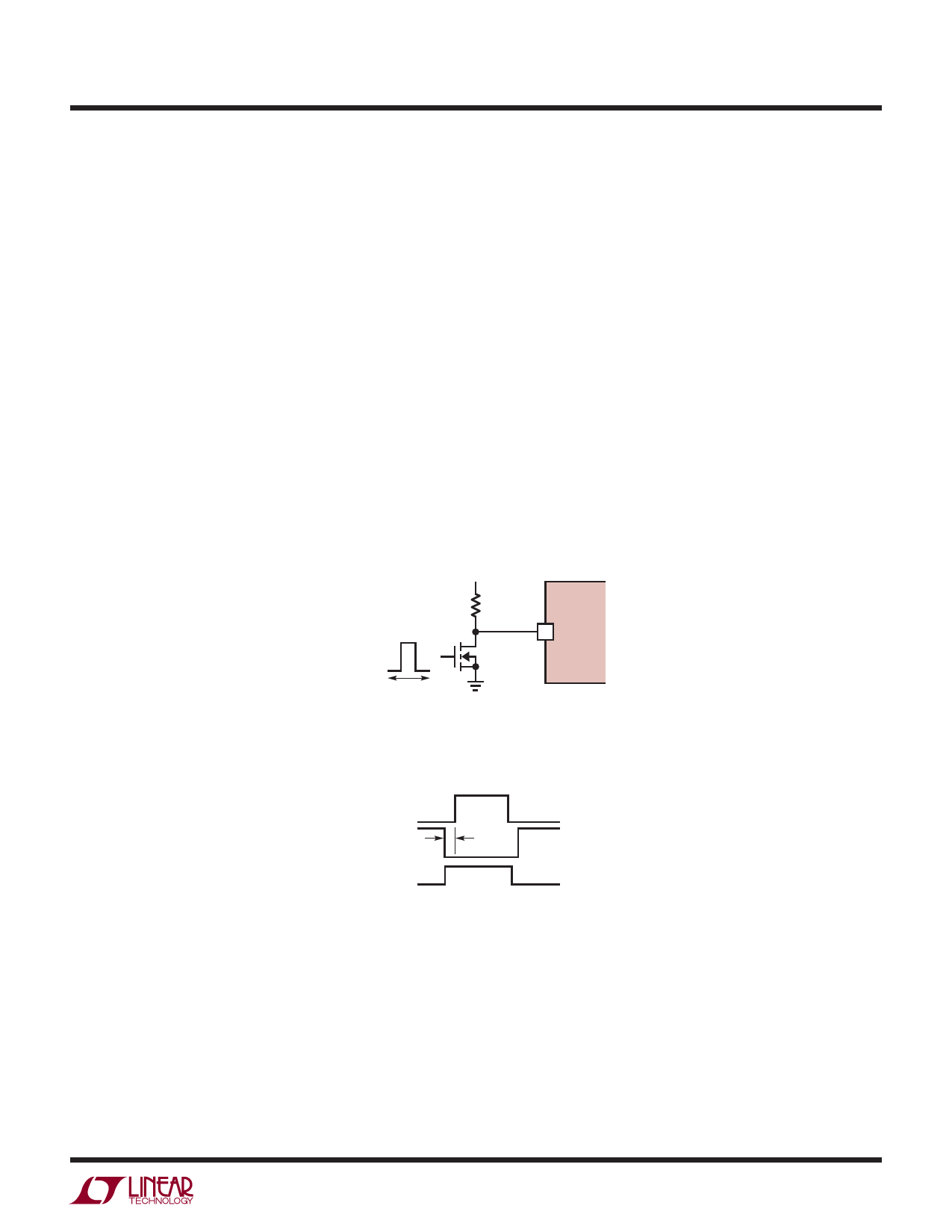
5V TO 20V
5k
SYNC
LT3782A
VN2222
PULSE WIDTH > 200ns
3782A F01
Figure 1. Synchronizing with External Clock
to drive external MOSFET drivers for synchronous recti-
fier operation. Note that SGATE drives the top switch and
BGATE drives the bottom switch. To avoid cross conduction
between top and bottom switches, the BGATE turn-on is
delayed 100ns (when DELAY pin is tied to RSET pin) from
SGATE turn-off (see Figure 2). If a longer delay is needed
to compensate for the propagation delay of external gate
driver, a resistor divider can be used from RSET to ground to
program VDELAY for the longer delay needed. For example,
for a switching frequency of 250kHz and delay of 150ns,
then RFREQ1 + RFREQ2 should be 80k and VDELAY should
be 1V, with VRSET = 2.3V then RFREQ1 = 47.5k and RFREQ2
= 32.5k (see Figure 3).
Duty Cycle Limit
When DCL pin is shorted to RSET pin and switching fre-
quency is less than 250kHz (RFREQ > 80k), the maximum
duty cycle of LT3782A will be at least 90%. The maximum
duty cycle can be clamped to 50% by grounding the DCL
pin or to 75% by forcing the VDCL voltage to 1.2V with a
resistor divider from RSET pin to ground. The typical DCL
pin input current is 0.1µA.
BGATE1
SGATE1 DELAY
SET
3782A F02
Figure 2. Delay Timing
DELAY
LT3782A
RFREQ1
47.5k
RSET
3782A F03
RFREQ2
32.5k
Figure 3. Increase Delay Time
For more information www.linear.com/LT3782A
3782afc
9
Share Link: 