LT3782EUFD Просмотр технического описания (PDF) - Linear Technology
Номер в каталоге
Компоненты Описание
Список матч
LT3782EUFD Datasheet PDF : 20 Pages
| |||
LT3782
APPLICATIONS INFORMATION
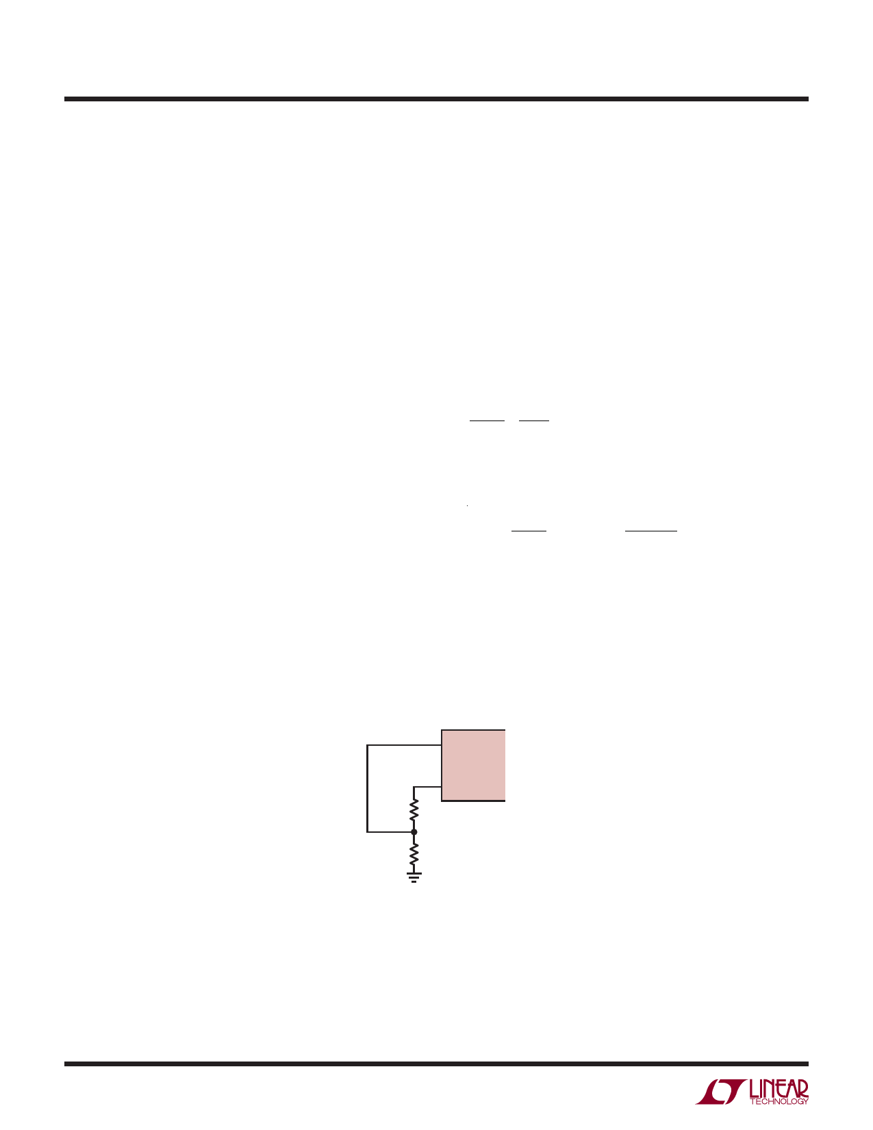
then RFREQ1 + RFREQ2 should be 80k and VDELAY should
be 1V, with VRSET = 2.3V then RFREQ1 = 47.5k and RFREQ2
= 32.5k (see Figure 3).
Duty Cycle Limit
When DCL pin is shorted to RSET pin and switching fre-
quency is less than 250kHz (RFREQ > 80k), the maximum
duty cycle of LT3782 will be at least 90%. The maximum
duty cycle can be clamped to 50% by grounding the DCL
pin or to 75% by forcing the VDCL voltage to 1.2V with a
resistor divider from RSET pin to ground. The typical DCL
pin input current is 0.2μA.
Slope Compensation
The LT3782 is designed for high voltage and/or high
current applications, and very often these applications
generate noise spikes that can be picked up by the cur-
rent sensing amplifier and cause switching jitter. To avoid
switching jitter, careful layout is absolutely necessary to
minimize the current sensing noise pickup. Sometimes
increasing slope compensation to overcome the noise
can help to reduce jitter. The built-in slope compensa-
tion can be increased by adding a resistor RSLOPE from
SLOPE pin to ground. Note that smaller RSLOPE increases
slope compensation and the minimum RSLOPE allowed is
RFREQ/2.
Layout Considerations
To prevent EMI, the power MOSFETs and input bypass
capacitor leads should be kept as short as possible. A
ground plane should be used under the switching circuitry
to prevent interplane coupling and to act as a thermal
spreading path. Note that the bottom pad of the package
is the heat sink, as well as the IC signal ground, and must
be soldered to the ground plane.
In a boost converter, the conversion gain (assuming 100%
efficiency) is calculated as (ignoring the forward voltage
drop of the boost diode):
VOUT = 1
VIN 1−D
where D is the duty ratio of the main switch. D can then
be estimated from the input and output voltages:
D = 1−
VIN
VOUT
;
DMAX
= 1−
VIN(MIN)
VOUT
RFREQ1
47.5k
RFREQ2
32.5k
DELAY
LT3782
RSET
3782 F03
Figure 3. Increase Delay Time
3782fg
10
Share Link: 