LT3029 Просмотр технического описания (PDF) - Linear Technology
Номер в каталоге
Компоненты Описание
Список матч
LT3029 Datasheet PDF : 20 Pages
| |||
LT3029
APPLICATIONS INFORMATION
Exercise care even when using X5R and X7R capacitors;
the X5R and X7R codes only specify operating temperature
range and maximum capacitance change over temperature.
Capacitance change due to DC bias (voltage coefficient)
with X5R and X7R capacitors is better than with Y5V and
Z5U capacitors, but can still be significant enough to drop
capacitor values below appropriate levels. Capacitor DC
bias characteristics tend to improve as case size increases.
Linear Technology recommends verifying expected versus
actual capacitance values at operating voltage in situ for
an application.
Voltage and temperature coefficients are not the only
sources of problems. Some ceramic capacitors have a
piezoelectric response. A piezoelectric device generates
voltage across its terminals due to mechanical stress,
similar to the way a piezoelectric accelerometer or micro-
phone works. For a ceramic capacitor, the stress can be
induced by vibrations in the system or thermal transients.
The resulting voltages produced can cause appreciable
amounts of noise, especially when a ceramic capacitor is
used for noise bypassing. A ceramic capacitor produced
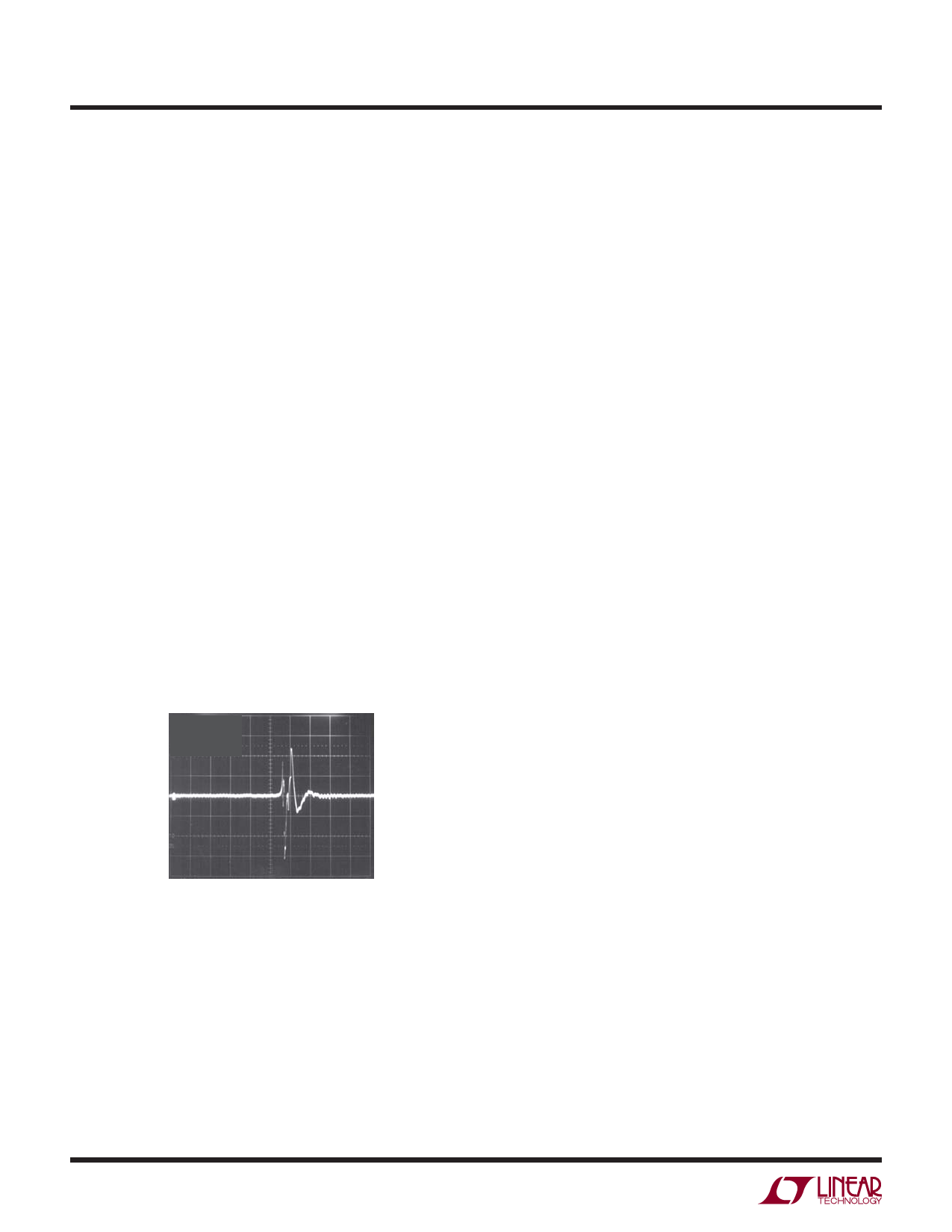
Figure 4’s trace in response to light tapping from a pencil.
Similar vibration induced behavior can masquerade as
increased output voltage noise.
COUT = 10μF
CBYP = 0.01μF
ILOAD = 500mA
VOUT
500μV/DIV
100ms/DIV
3029 F04
Figure 4. Noise Resulting from Tapping on a Ceramic Capacitor
Thermal Considerations
The LT3029’s power handling capability limits the maximum
rated junction temperature (125°C, LT3029E/LT3029I/
LT3029MP or 150°C, LT3029H). Two components comprise
the power dissipated by each channel:
1. Output current multiplied by the input/output voltage
differential: (IOUT)(VIN – VOUT), and
2. GND pin current multiplied by the input voltage:
(IGND)(VIN).
Ground pin current is found by examining the GND Pin
Current curves in the Typical Performance Characteristics
section.
Power dissipation for each channel equals the sum of the
two components listed above. Total power dissipation for
the LT3029 equals the sum of the power dissipated by
each channel.
The LT3029’s internal thermal shutdown circuitry protects
both channels of the device if either channel experiences
an overload or fault condition. Activation of the thermal
shutdown circuitry turns both channels off. If the overload
or fault condition is removed, both outputs are allowed
to turn back on. For continuous normal conditions, do
not exceed the maximum junction temperature rating of
125°C (LT3029E/LT3029I/LT3029MP) or 150°C (LT3029H).
Carefully consider all sources of thermal resistance from
junction-to-ambient, including additional heat sources
mounted in proximity to the LT3029. For surface mount
devices, use the heat spreading capabilities of the PC board
and its copper traces to accomplish heat sinking. Copper
board stiffeners and plated through-holes can also spread
the heat generated by power devices.
The following tables list thermal resistance as a function
of copper area in a fixed board size. All measurements
were taken in still air on a four-layer FR-4 board with 1oz
solid internal planes, and 2oz external trace planes with a
total board thickness of 1.6mm. For further information
on thermal resistance and using thermal information, refer
to JEDEC standard JESD51, notably JESD51-12.
3029fa
14
Share Link: 