LT3027 Просмотр технического описания (PDF) - Linear Technology
Номер в каталоге
Компоненты Описание
Список матч
LT3027
Linear Technology

LT3027 Datasheet PDF : 16 Pages
| |||
LT3027
APPLICATIO S I FOR ATIO
Voltage and temperature coefficients are not the only
sources of problems. Some ceramic capacitors have a
piezoelectric response. A piezoelectric device generates
voltage across its terminals due to mechanical stress,
similar to the way a piezoelectric accelerometer or
microphone works. For a ceramic capacitor the stress
can be induced by vibrations in the system or thermal
transients. The resulting voltages produced can cause
appreciable amounts of noise, especially when a ceramic
capacitor is used for noise bypassing. A ceramic capaci-
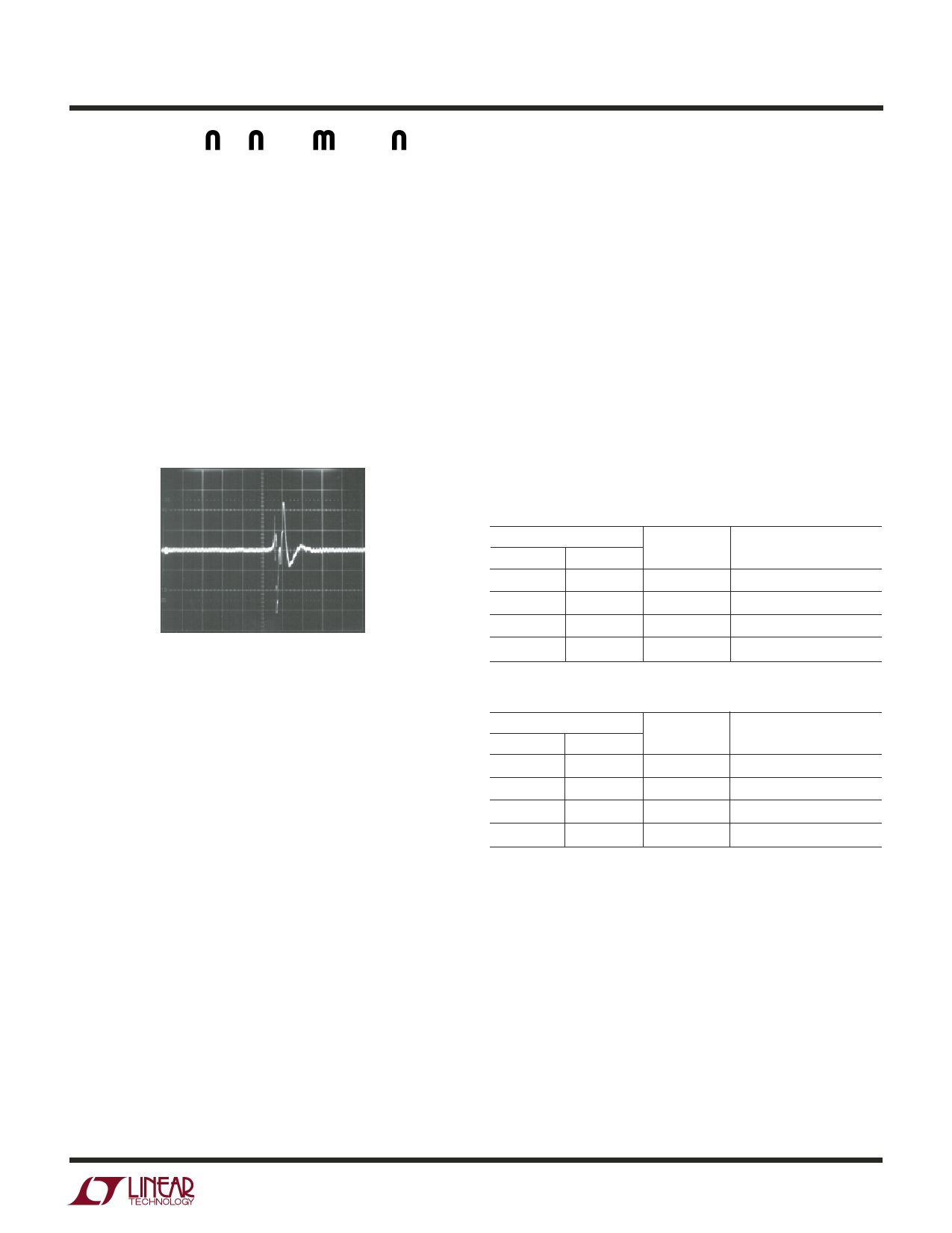
tor produced Figure 5’s trace in response to light tapping
from a pencil. Similar vibration induced behavior can
masquerade as increased output voltage noise.
COUT = 10µF
CBYP = 0.01µF
ILOAD = 100mA
VOUT
500µV/DIV
100ms/DIV
3027 F05
Figure 5. Noise Resulting from Tapping on a Ceramic Capacitor
Thermal Considerations
The power handling capability of the device will be limited
by the maximum rated junction temperature (125°C). The
power dissipated by the device will be made up of two
components (for each channel):
1. Output current multiplied by the input/output voltage
differential: (IOUT)(VIN – VOUT), and
2. GND pin current multiplied by the input voltage:
(IGND)(VIN).
The ground pin current can be found by examining the
GND Pin Current curves in the Typical Performance
Characteristics section. Power dissipation will be equal to
the sum of the two components listed above. Power
dissipation from both channels must be considered dur-
ing thermal analysis.
The LT3027 regulator has internal thermal limiting de-
signed to protect the device during overload conditions.
For continuous normal conditions, the maximum junction
temperature rating of 125°C must not be exceeded. It is
important to give careful consideration to all sources of
thermal resistance from junction to ambient. Additional
heat sources mounted nearby must also be considered.
For surface mount devices, heat sinking is accomplished
by using the heat spreading capabilities of the PC board
and its copper traces. Copper board stiffeners and plated
through-holes can also be used to spread the heat gener-
ated by power devices.
The following tables list thermal resistance for several
different board sizes and copper areas. All measurements
were taken in still air on 3/32" FR-4 board with one ounce
copper.
Table 1. MSE Package, 10-Lead MSOP
COPPER AREA
THERMAL RESISTANCE
TOPSIDE* BACKSIDE BOARD AREA (JUNCTION-TO-AMBIENT)
2500mm2
1000mm2
225mm2
100mm2
2500mm2
2500mm2
2500mm2
2500mm2
2500mm2
2500mm2
2500mm2
2500mm2
40°C/ W
45°C/ W
50°C/ W
62°C/ W
*Device is mounted on topside.
Table 2. DD Package, 10-Lead DFN
COPPER AREA
THERMAL RESISTANCE
TOPSIDE* BACKSIDE BOARD AREA (JUNCTION-TO-AMBIENT)
2500mm2
1000mm2
225mm2
100mm2
2500mm2
2500mm2
2500mm2
2500mm2
2500mm2
2500mm2
2500mm2
2500mm2
40°C/ W
45°C/ W
50°C/ W
62°C/ W
*Device is mounted on topside.
The thermal resistance juncton-to-case (θJC), measured
at the Exposed Pad on the back of the die is 10°C/W.
Calculating Junction Temperature
Example: Given an output voltage on the first channel of
3.3V, an output voltage of 2.5V on the second channel, an
input voltage range of 4V to 6V, output current ranges of
0mA to 100mA for the first channel and 0mA to 50mA for
the second channel, with a maximum ambient tempera-
ture of 50°C, what will the maximum junction temperature
be?
3027f
11
Share Link: