LAN9118 Просмотр технического описания (PDF) - SMSC -> Microchip
Номер в каталоге
Компоненты Описание
Список матч
LAN9118 Datasheet PDF : 129 Pages
| |||
High Performance Single-Chip 10/100 Non-PCI Ethernet Controller
Datasheet
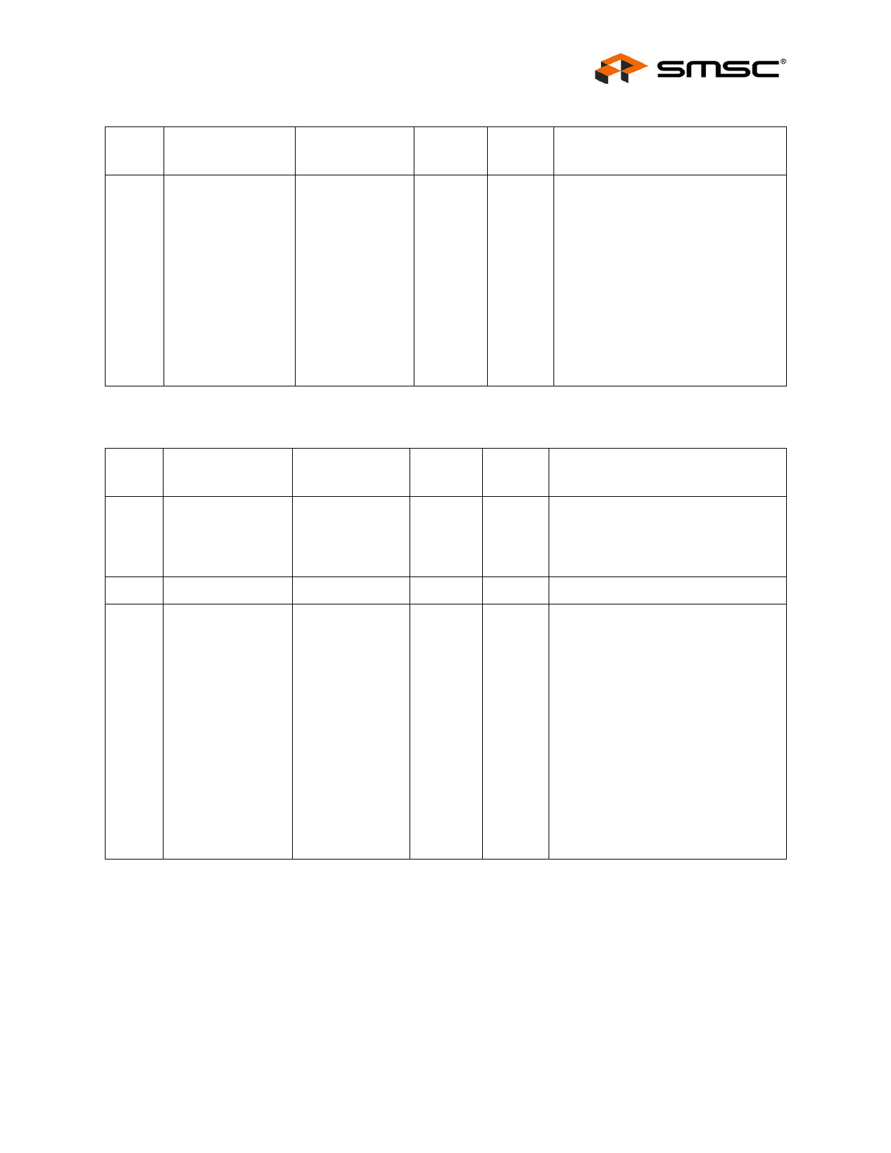
Table 2.4 Serial EEPROM Interface Signals (continued)
PIN
NO.
NAME
SYMBOL
BUFFER
TYPE
NUM
PINS
DESCRIPTION
69
EEPROM Clock, EECLK/GPO4/
O8
GPO4 RX_DV, RX_DV/RX_CLK
RX_CLK
1
EEPROM Clock: Serial EEPROM
Clock pin.
General Purpose Output 4: This
pin can also function as a general-
purpose output, or it can be
configured to monitor the RX_DV or
RX_CLK signals on the internal MII
port. When configured as a GPO
signal, or as an RX_DV/RX_CLK
monitor, the EECS pin is deasserted
so as to never unintentionally access
the serial EEPROM. This signal
cannot function as a general-
purpose input.
PIN
NO.
NAME
6
Crystal 1
5
Crystal 2
95
Reset
Table 2.5 System and Power Signals
SYMBOL
XTAL1
XTAL2
nRESET
BUFFER NUM
TYPE
PINS
lclk
1
Oclk
1
IS
1
(PU)
DESCRIPTION
External 25MHz Crystal Input.
Can also be connected to single-
ended TTL oscillator. If this method is
implemented, XTAL2 should be left
unconnected.
External 25MHz Crystal output.
Active-low reset input. Resets all logic
and registers within the LAN9118
This signal is pulled high with a weak
internal pull-up resistor. If nRESET is
left unconnected, the LAN9118 will
rely on its internal power-on reset
circuitry
Note:
The LAN9118 must always
be read at least once after
power-up, reset, or upon
return from a power-saving
state or write operations will
not function. See Section
3.11, "Detailed Reset
Description," on page 41 for
additional information
SMSC LAN9118
17
DATASHEET
Revision 1.3 (05-31-07)
Share Link: 