LA8519M Просмотр технического описания (PDF) - SANYO -> Panasonic
Номер в каталоге
Компоненты Описание
Список матч
LA8519M Datasheet PDF : 29 Pages
| |||
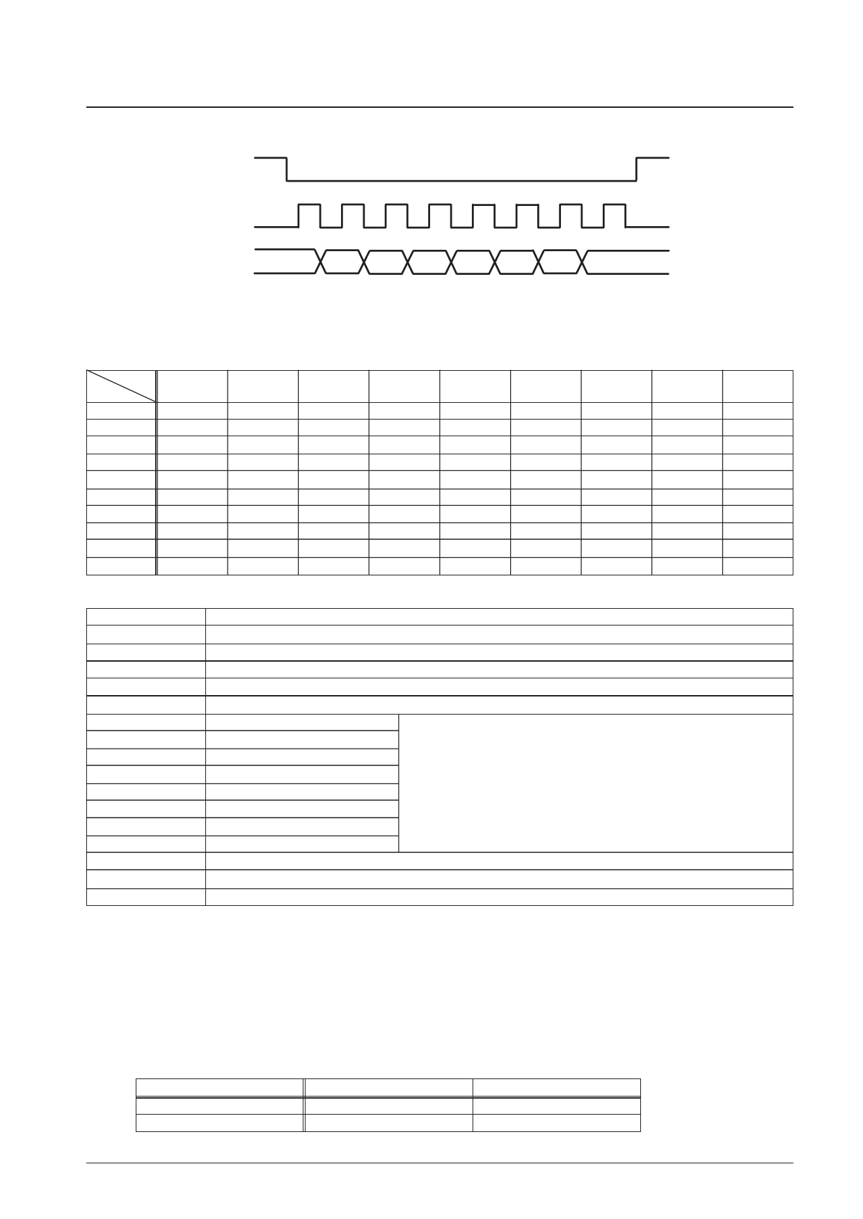
Serial Data Format
CE
CLOCK
LA8519M
DATA
A6 A5 A4
A3
A2
A1
A0
D
A6 to A0 ⇒ Sets the address of the crosspoint switch or control switch (hexadecimal ⇒ binary number)
D⇒
Sets the on/off state of the crosspoint switch or control switch.
(The switch is set to the on state when D is 1, and to the off state when 0.)
Address Table
Output
LINE
HAND
RF1
Input
LINE
—
08
10
HAND
01
—
11
RF1
02
09
—
RF2
03
0A
12
DOOR
—
0B
13
CDC1
04
0C
14
CDC2
05
0D
15
MIC
—
—
—
BEEP
06
0E
16
PRE
07
0F
—
RF2
DOOR
CDC1
CDC2
EVR
17
—
24
2B
32
18
1E
25
2C
—
19
1F
26
2D
—
—
20
27
2E
—
1A
—
28
2F
—
1B
21
—
—
33
1C
22
—
—
34
—
—
29
30
—
1D
23
—
—
35
—
—
2A
31
36
PRE
37
38
—
—
—
39
3A
3B
—
—
Other addresses
Address No.
00
3C
3D
3E
3F
40
41
42
43
44
45
46
47
7D
7E
7F
Mode
Sets all crosspoint and control switches to the off state. *2
ALC control (D = 1: Off, D = 0: On)
Transmitter/receiver control (SW1 and SW4 in the block diagram) *1
OSC input (SW5) control (D = 1: On, D = 0: Off)
Power amplifier control (D = 1: On, D = 0: Off)
Electronic volume control
0 dB
⇒ (Default value)
Electronic volume control –4 dB
Electronic volume control –8 dB
Electronic volume control –12 dB *2
Electronic volume control –16 dB
Electronic volume control –20 dB
Electronic volume control –24 dB
Electronic volume control –28 dB
Line attenuator (L-ATT) setting (D = 1: –6 dB, D = 0: 0 dB)
Receiver attenuator (R-ATT) setting (D = 1: 0 dB, D = 0: –6 dB)
Oscillator attenuator (OSC-ATT) setting (D = 1: 0 dB, D = 0: –16 dB)
* With address 3D set to the on state, SW1 is set to enable the transmitter amplifier output (pin 42) and SW4 is set to enable either the receiver amplifier
output (pin 55) or the KT (pin 39) signal. If a voltage is not supplied to VCC (pin 17) (i.e. the power off state), SW1 and SW4 are set to the same states
as when address 3D is set to the on state.
** For addresses 00 and 40 to 47, the data D may be either 0 or 1.
Notes: 1. The receiver attenuator (R-ATT) is set to –6 dB at power on or after a reset (pin 33 set to low, or address 00 accessed).
2. The line attenuator (L-ATT) is set to 0 dB at power on or after a reset (pin 33 set to low, or address 00 accessed).
3. The oscillator attenuator (OSC-ATT) is set to –16 dB at power on or after a reset (pin 33 set to low, or address 00 accessed).
4. The electronic volume control is set to 0 dB at power on or after a reset (pin 33 set to low, or address 00 accessed).
5. Addresses are expressed as hexadecimal numbers.
6. Since the LA8519M includes a power on reset function, all the crosspoint and control switches are reset to their default states when external power
(pin 17: VCC) is applied.
7. Switches SW2 and SW3 in the block diagram are controlled by the MUTE pin (pin 35). The table lists the signals enabled by this pin.
MUTE pin (pin 35)
High/Open
Low
SW2
Transmitter (pin 42) and TA-IN (pin 43)
DTMF pin (pin 44)
SW3
Receiver (pin 55)
KT pin (pin 39)
No. 6471-8/29
Share Link: 