AD8345(REV0) Просмотр технического описания (PDF) - Analog Devices
Номер в каталоге
Компоненты Описание
Список матч
AD8345 Datasheet PDF : 16 Pages
| |||

AD8345
10k⍀
1.5k⍀
348⍀
IIN
49.9⍀
348⍀
24.9⍀
+5V
348⍀
0.1F 10F 0.01F 1000pF
1000pF 0.01F
0.1F
AD8132
348⍀
IBBP
IBBN
VPS1 VPS2
VOUT
⌺
–5V
+5V
0.1F
10F
348⍀
0.1F 10F
348⍀
QIN
49.9⍀
348⍀
0.1F
AD8132
QBBP
PHASE
SPLITTER
LOIP
LOIN
QBBN
AD8345
COM1 COM2 COM3
24.9⍀
348⍀
10F 0.1F
–5V
Figure 5. Single-Ended IQ Drive Circuit
The I and Q inputs have high input impedances because they
connect directly to the bases of pnp transistors. If a (dc-coupled)
filter is being used between a DAC and the modulator inputs,
this filter will need to be terminated with the appropriate resis-
tance. If the filter is differential, the termination resistor should
be connected across the I and Q differential inputs.
Reduction of LO Leakage
Because the I and Q signals are being effectively multiplied with
the LO, any internal offset voltages on these inputs will result in
leakage of the LO. The nominal LO leakage of –42 dBm which
results from these internal offset voltages, can be reduced further
by applying offset compensation voltages on the I and Q inputs.
(Note that LO feedthrough is reduced by varying the differential
offset voltages on the I and Q inputs, not by varying the nominal
bias level of 0.7 V.) This is easily accomplished by programming
(and then storing) the appropriate DAC offset code to reduce
the LO leakage. This does, however, require the path from the
DAC to the I and Q inputs to be dc-coupled. (DC-coupling is
also advantageous from the perspective of I and Q input bias-
ing if the DAC is capable of delivering a bias level of 0.7 V).
The procedure for reducing the LO feedthrough is simple. In
order to isolate the LO in the output spectrum, a single side-
band configuration is recommended (set I and Q signals to sine
and cosine waves at, say, 100 kHz, set LO to FRF – 100 kHz).
An offset voltage is applied from the I DAC until the LO leakage
reaches a trough. With this offset level held, an offset voltage is
applied to the Q DAC until a (lower) trough is reached.
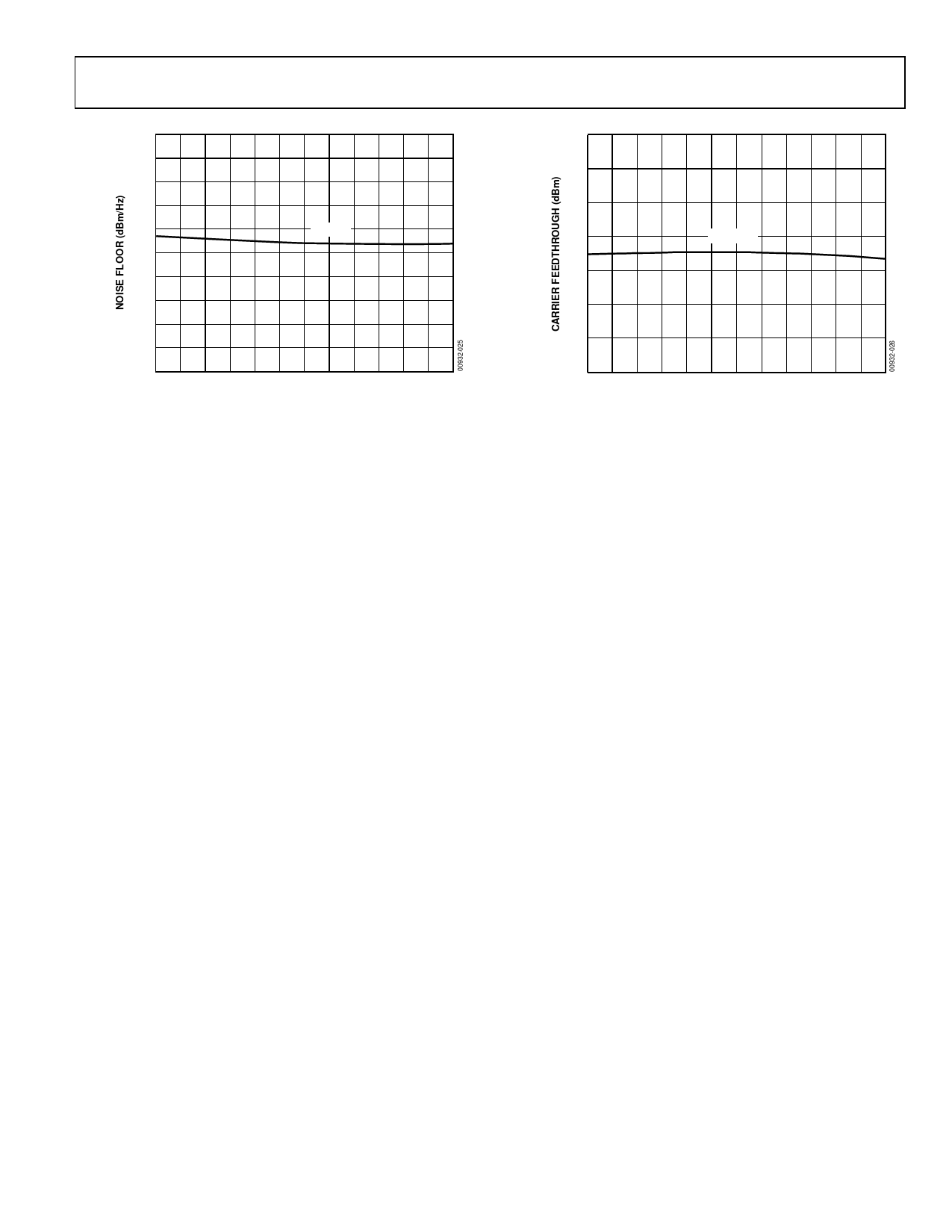
LO leakage compensation holds up well over temperature. TPC
8 shows the effect of temperature on LO leakage after compen-
sation at ambient.
Compensated LO leakage will degrade somewhat as the frequency
is moved away from the frequency at which the compensation
was performed. This is due to the effects of LO to RF output
leakage which are not a result of offsets on the I and Q inputs.
Single-Ended I and Q Drive
Where only single-ended I and Q signals are available, a differ-
ential amplifier such as the AD8132 or AD8138 can be used to
generate the required differential drive signal for the AD8345.
Even though most DACs have differential outputs, using a
single-ended low-pass filter between the dual DAC and the I
and Q inputs, may be more desirable from the perspective of
component count and cost. As a result, the output signal from
the filter must be converted back to differential mode and possi-
bly be rebiased to 0.7 V common mode.
Figure 5 shows a circuit which converts a ground-referenced,
single-ended signal to a differential signal and adds the required
0.7 V bias voltage. Two AD8132 differential op amps, config-
ured for a gain of unity, are used. With a 50 Ω input impedance,
this circuit is configured to accept a signal from a 50 Ω source
(e.g., a low-pass filter). The input impedance can be easily changed
by replacing the 49.9 Ω shunt resistor (and the corresponding
24.9 Ω resistor on the inverting input) with the appropriate value.
The required dc-bias level is conveniently added to the signal by
applying 0.7 V to the VOCM pins of the differential amplifiers.
Differential amplifiers such as the AD8132 and AD8138 can
also be used to implement active filters. For more information
on this topic, consult the data sheets of these devices.
–10–
REV. 0