L4955 Просмотр технического описания (PDF) - STMicroelectronics
Номер в каталоге
Компоненты Описание
Список матч
L4955 Datasheet PDF : 14 Pages
| |||
L4955
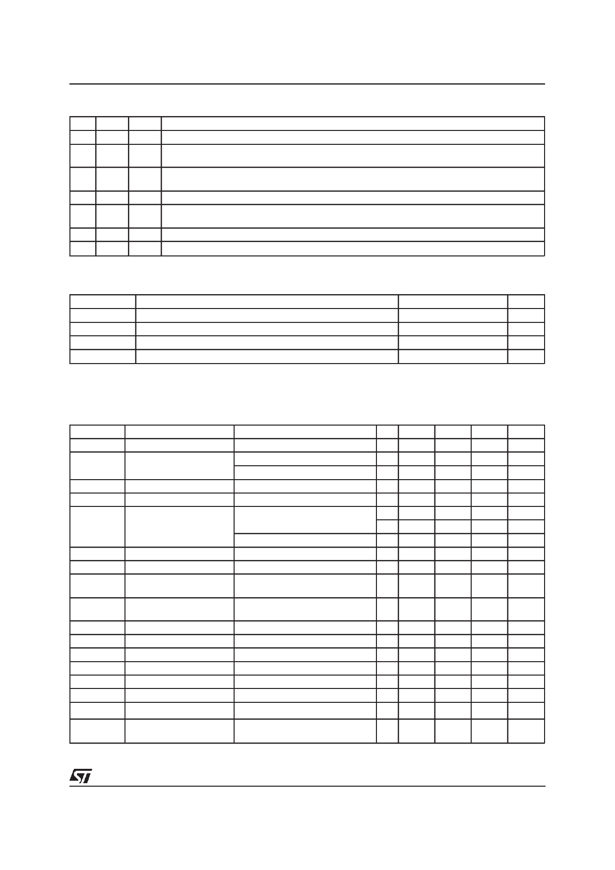
PIN FUNCTIONS
HW VW Name
Fun ction
1
1
IN Unregulated input voltage; this pin must be bypassed with a capacitor larger than 10µF.
2
–
CL A resistor connected between this pin and ground sets the programmable current limiting
value. When the programmable current limiting is not used the pin must be connected to GND.
3
– INH TTL-CMOS input. A logic high level on this input disables the device. An internal pull-down
insures full functionally even if the pin is open.
4
2 GND Ground.
5
– ADJ The output is connected directly to this terminal for 1.26V operation; it is connected to the
output through a resistive divider for higher voltages.
6
–
PG Open drain output, this signal is low when the output voltage is lower than 90%, otherwise is high.
7
3 OUT Regulated output voltage. A minimum bypass capacitor of 22µF is required to insure stability.
THERMAL DATA (HEPTAWATT & VERSAWATT packages)
Symbol
Rth j-case
Rth j-amb
Parameter
Thermal Resistance Junction-case
Thermal Resistance Junction-ambient
Thermal Shutdown
Thermal Hysteresis
Max.
Max.
Typ.
Typ.
Value
2.5
50
150
20
Unit
°C/W
°C/W
°C
°C
L•4=9S55pe-cEifLicEaCtioTnRsICreAfeLrrCeHd AtoRTAJCfrToEmR0IS°CTItCoS+1(T2j5=°C2.5°C, Vin = 12V, unless otherwise specified).
Symbol
VIN
VO
Parameter
Operating Supply Voltage
Output Voltage (1)
∆VO
Line regulation (1)
∆VO
Load regulation (1)
VO
Dropout Voltage
IO
Current Limiting
Short Circuit Current
Programmable Current
Limiting
IQ
Quiescent Current
Stand By Current
Inhibit Threshold
Inhibit Hysteresis
Inhibit Bias Sink Current
Power Good Threshold
Power Good Hysteresis
Power Good Saturation
Ripple Rejection
(1) Output voltage connected to ADJ.
Test Condition
0.1A < IO < 5A; 4.5V < VIN <12V
4.5V < VIN < 12V; 0.1A < IO < 5A
4.5V < VIN <22V; IO = 10mA
0.1A < IO < 5A
IO = 5A
VIN ≥ 4.5V
IO = 2A
VO = 0V
Rlim = 13kΩ
Rlim = 47kΩ
0.1A < IO < 5A
INH = 5V
Rising Edge
CL = 0
CL = 13k
INH = 5V or 0.8V
Rising Edge
IPG = 4mA
f = 120Hz, IO = 5A
VIN = 6V ∆VIN = 2VPP
Min. Typ. Max.
4.5
22
1.235 1.26 1.285
• 1.222 1.26 1.298
2
10
2
10
0.75 1.1
•
1.1
1.5
•
0.55 0.75
• 5.1
6.3
7.5
•
1.8
• 2.55
3
3.45
• 0.70 0.85 1.00
2
3
2.7
4
120 200
• 1.1 1.26 1.42
0.2
20
60
0.9 x VO
•
0.2
•
0.1
0.4
60
75
Unit
V
V
V
mV
mV
V
V
V
A
A
A
A
mA
mA
µA
V
V
µA
V
V
V
dB
3/14
Share Link: 