L4901 Просмотр технического описания (PDF) - STMicroelectronics
Номер в каталоге
Компоненты Описание
Список матч
L4901 Datasheet PDF : 10 Pages
| |||
L4901A
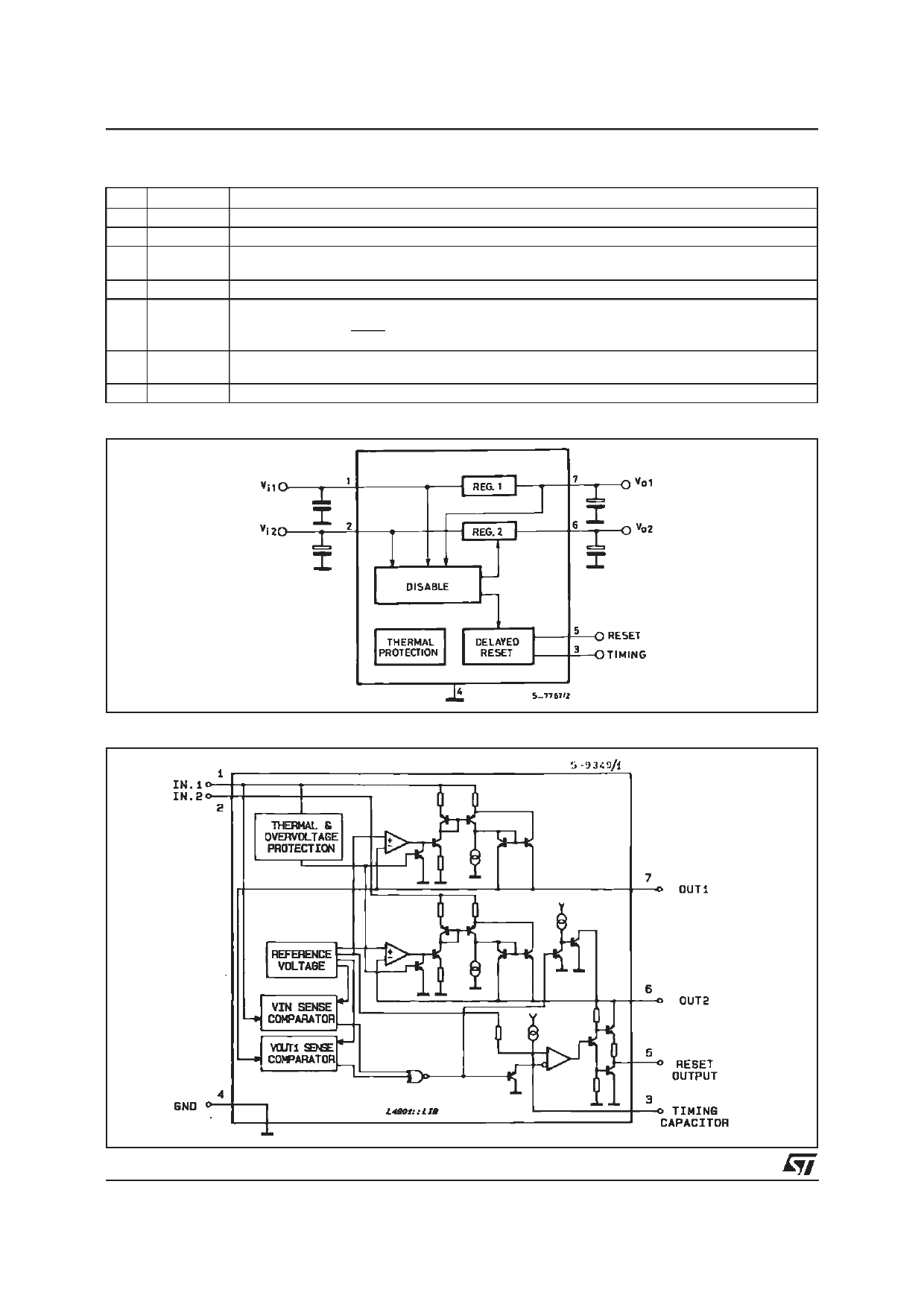
PIN DESCRIPTION
N°
Name
Fun ction
1
Input 1 Low Quiescent Current 400mA Regulator Input.
2
Input 2 400mA regulator input.
3
Timing If Reg. 2 is switched-ON the delay capacitor is charged with a 10µA constant current. When Reg.
Capacitor 2 is switched-OFF the delay capacitor is decharged.
4
GND Common Ground.
5
Reset When pin 3 reaches 5V the reset output is switched high.
Output
Therefore
tRD
=
Ct
( 5V );
10µA
tRD (ms) = Ct (nF)
6 Output 2 5V – 400mA Regulator Output. Enabled if Vo 1 > VRT and VIN 2 > VIT. If Reg. 2 is switched-OFF
the C02 capacitor is discharged.
7 Output 1 5V – 400mA regulator output with Low leakage (in switch-OFF condition).
BLOCK DIAGRAM
SCHEMATIC DIAGRAM
2/10
Share Link: 