RT9168-15CBR Просмотр технического описания (PDF) - Richtek Technology
Номер в каталоге
Компоненты Описание
Список матч
RT9168-15CBR Datasheet PDF : 11 Pages
| |||
RT9168/A
To ensure proper operation, the signal source used to
drive the EN input must be able to swing above and below
the specified turn-on/turn-off voltage thresholds which
guarantee an ON or OFF state (see Electrical Characteristics).
The ON/OFF signal may come from either CMOS output,
or an open-collector output with pull-up resistor to the
RT9168/A input voltage or another logic supply. The high-
level voltage may exceed the RT9168/A input voltage,
but must remain within the absolute maximum ratings
for the EN pin.
Internal P-Channel Pass Transistor
The RT9168/A features a typical 1.1Ω P-channel MOSFET
pass transistor. It provides several advantages over similar
designs using PNP pass transistors, including longer
battery life. The P-channel MOSFET requires no base
drive, which reduces quiescent current considerably. PNP-
based regulators waste considerable current in dropout
when the pass transistor saturates. They also use high
base-drive currents under large loads. The RT9168/A does
not suffer from these problems and consume only 80μA of
quiescent current whether in dropout, light-load, or heavy-
load applications.
Input-Output (Dropout) Voltage
A regulator's minimum input-output voltage differential (or
dropout voltage) determines the lowest usable supply
voltage. In battery-powered systems, this will determine
the useful end-of-life battery voltage. Because the
RT9168/A uses a P-channel MOSFET pass transistor,
the dropout voltage is a function of drain-to-source on-
resistance [RDS(ON)] multiplied by the load current.
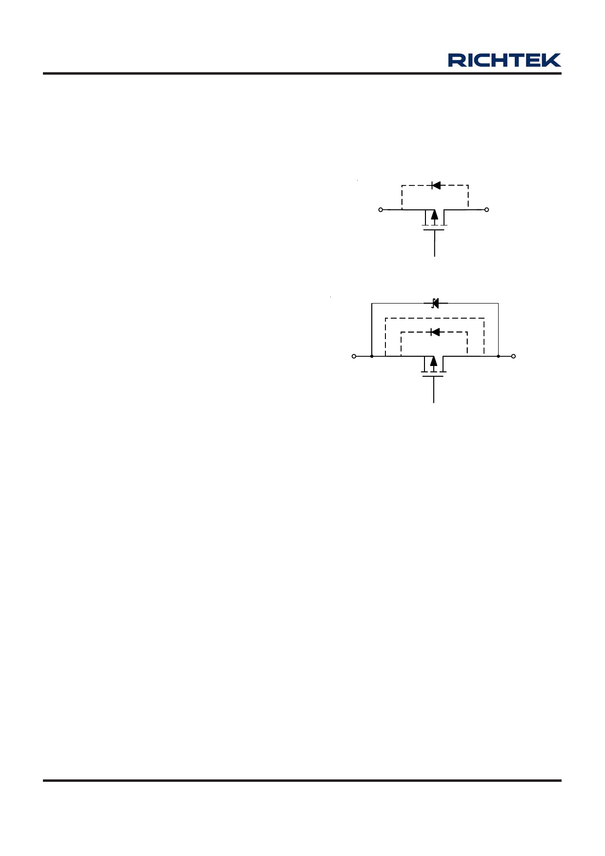
Reverse Current Path
The power transistor used in the RT9168/A has an inherent
diode connected between the regulator input and output
(see Figure 2). If the output is forced above the input by
more than a diode-drop, this diode will become forward
biased and current will flow from the VOUT terminal to VIN.
This diode will also be turned on by abruptly stepping the
input voltage to a value below the output voltage. To prevent
regulator mis-operation, a Schottky diode should be used
in any applications where input/output voltage conditions
can cause the internal diode to be turned on (see Figure
3). As shown, the Schottky diode is connected in parallel
with the internal parasitic diode and prevents it from being
turned on by limiting the voltage drop across it to about
0.3V. < 100 mA to prevent damage to the part.
VIN
VOUT
Figure 2
VIN
VOUT
Figure 3
Current Limit and Thermal Protection
The RT9168 includes a current limit which monitors and
controls the pass transistor's gate voltage limiting the
output current to 300mA Typ. (700mA Typ. for RT9168A).
Thermal-overload protection limits total power dissipation
in the RT9168/A. When the junction temperature exceeds
TJ = +155°C, the thermal sensor signals the shutdown
logic turning off the pass transistor and allowing the IC to
cool. The thermal sensor will turn the pass transistor on
again after the IC's junction temperature cools by 10°C,
resulting in a pulsed output during continuous thermal-
overload conditions. Thermal-overloaded protection is
designed to protect the RT9168/A in the event of fault
conditions. Do not exceed the absolute maximum
junction-temperature rating of TJ = +150°C for continuous
operation. The output can be shorted to ground for an
indefinite amount of time without damaging the part by
cooperation of current limit and thermal protection.
www.richtek.com
8
DS9168/A-15 March 2007
Share Link: 