K4E641611D-TC50 Просмотр технического описания (PDF) - Samsung
Номер в каталоге
Компоненты Описание
Список матч
K4E641611D-TC50 Datasheet PDF : 36 Pages
| |||
K4E661611D, K4E641611D
CMOS DRAM
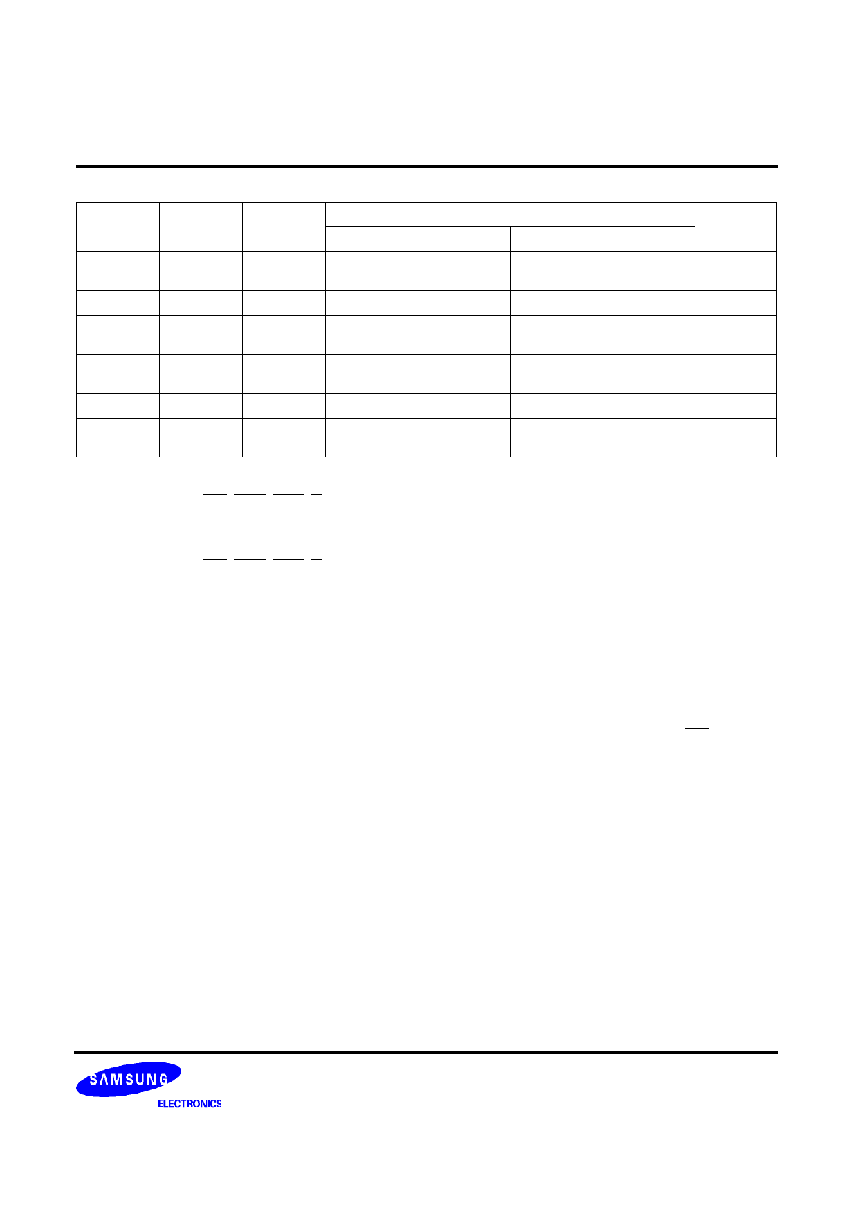
DC AND OPERATING CHARACTERISTICS (Continued)
Symbol
Power
Speed
K4E661611D
Max
ICC1
Don′t care
-50
-60
90
80
ICC2
Normal
Don′t care
2
ICC3
Don′t care
-50
-60
90
80
ICC4
Don′t care
-50
-60
100
90
ICC5
Normal
Don′t care
1
ICC6
Don′t care
-50
-60
120
110
K4E641611D
120
110
2
120
110
110
100
1
120
110
Units
mA
mA
mA
mA
mA
mA
mA
mA
mA
mA
ICC1* : Operating Current (RAS and UCAS, LCAS, Address cycling @tRC=min.)
ICC2 : Standby Current (RAS=UCAS=LCAS=W=VIH)
ICC3* : RAS-only Refresh Current (UCAS=LCAS=VIH, RAS, Address cycling @tRC=min.)
ICC4* : Extended Data Out Mode Current (RAS=VIL, UCAS or LCAS, Address cycling @tHPC=min.)
ICC5 : Standby Current (RAS=UCAS=LCAS=W=VCC-0.2V)
ICC6* : CAS-Before-RAS Refresh Current (RAS and UCAS or LCAS cycling @tRC=min)
*Note : ICC1, ICC3, ICC4 and ICC6 are dependent on output loading and cycle rates. Specified values are obtained with the output open.
ICC is specified as an average current. In ICC1, ICC3 and ICC6, address can be changed maximum once while RAS=VIL. In ICC4,
address can be changed maximum once within one EDO mode cycle time tHPC.
Share Link: 